
SLIDE 1
Principles of VLSI Design Performance Estimation CMSC 491B/711 1 (November 26, 2000 7:49 pm)
UMBC
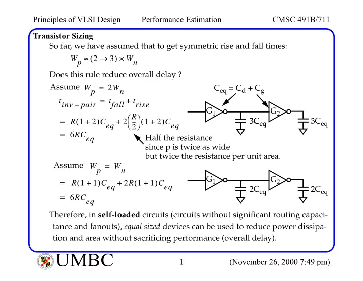
U M B C U N I V E R S I T Y O F M A R Y L A N D B A L T I M O R E C O U N T Y 1 9 6 6Transistor Sizing So far, we have assumed that to get symmetric rise and fall times: Does this rule reduce overall delay ? Therefore, in self-loaded circuits (circuits without significant routing capaci- tance and fanouts), equal sized devices can be used to reduce power dissipa- tion and area without sacrificing performance (overall delay). Wp 2 3 → ( ) Wn × ≈ Wp 2Wn = Assume G1 G2 3Ceq 3Ceq Wp Wn = Assume G1 G2 2Ceq 2Ceq tinv pair – tfall trise + = 3Ceq Ceq = Cd + Cg R 1 2 + ( )Ceq 2 R 2
-
1 2 + ( )Ceq + = = 6RCeq R 1 1 + ( )Ceq 2R 1 1 + ( )Ceq + = = 6RCeq Half the resistance since p is twice as wide but twice the resistance per unit area.