
SLIDE 1
VLSI Design Verification and Test Overview I CMPE 646 1 (11/1/04)
UMBC
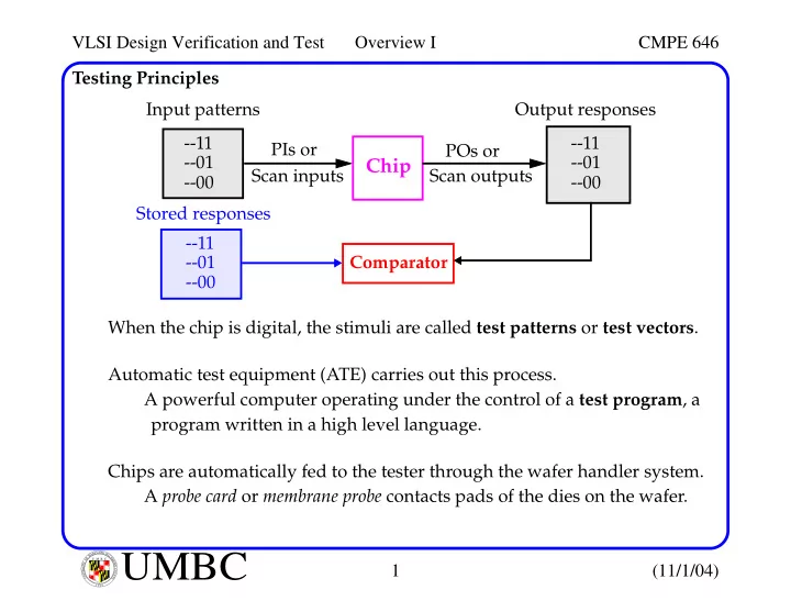
U M B C U N I V E R S I T Y O F M A R Y L A N D B A L T I M O R E C O U N T Y 1 9 6 6Testing Principles When the chip is digital, the stimuli are called test patterns or test vectors. Automatic test equipment (ATE) carries out this process. A powerful computer operating under the control of a test program, a program written in a high level language. Chips are automatically fed to the tester through the wafer handler system. A probe card or membrane probe contacts pads of the dies on the wafer. Input patterns
Chip
PIs or Scan inputs POs or Scan outputs
- -11
- -01
- -00
Output responses
- -11
- -01
- -00
Stored responses Comparator
- -11
- -01
- -00