
SLIDE 1
VLSI Design Verification and Test Combo ATPG II CMPE 646 1 (10/21/04)
UMBC
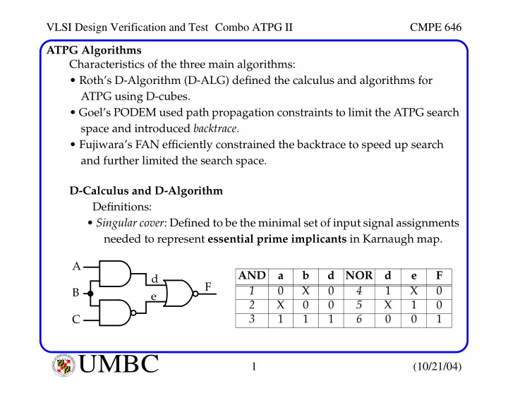
U M B C U N I V E R S I T Y O F M A R Y L A N D B A L T I M O R E C O U N T Y 1 9 6 6ATPG Algorithms Characteristics of the three main algorithms:
- Roth’s D-Algorithm (D-ALG) defined the calculus and algorithms for
ATPG using D-cubes.
- Goel’s PODEM used path propagation constraints to limit the ATPG search
space and introduced backtrace.
- Fujiwara’s FAN efficiently constrained the backtrace to speed up search
and further limited the search space. D-Calculus and D-Algorithm Definitions:
- Singular cover: Defined to be the minimal set of input signal assignments
needed to represent essential prime implicants in Karnaugh map. A C B d e F AND a b d NOR d e F 1 X 4 1 X 2 X 5 X 1 3 1 1 1 6 1