
SLIDE 1
Systems Design & Programming 8086/88 Chip Set CMPE 310 1 (Feb. 20, 2002)
UMBC
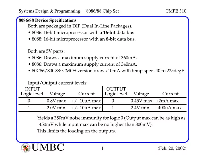
U M B C U N I V E R S I T Y O F M A R Y L A N D B A L T I M O R E C O U N T Y 1 9 6 68086/88 Device Specifications Both are packaged in DIP (Dual In-Line Packages).
- 8086: 16-bit microprocessor with a 16-bit data bus
- 8088: 16-bit microprocessor with an 8-bit data bus.
Both are 5V parts:
- 8086: Draws a maximum supply current of 360mA.
- 8086: Draws a maximum supply current of 340mA.
- 80C86/80C88: CMOS version draws 10mA with temp spec -40 to 225degF.
Input/Output current levels: Yields a 350mV noise immunity for logic 0 (Output max can be as high as 450mV while input max can be no higher than 800mV). This limits the loading on the outputs. Logic level Voltage Current 0.8V max +/- 10uA max 1 2.0V min +/- 10uA max Logic level Voltage Current 0.45V max +2mA max 1 2.4V min
- 400uA max
INPUT OUTPUT