
Digital Systems Transmission Lines III CMPE 650 1 (3/18/08)
UMBC
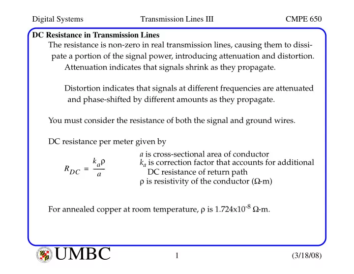
U M B C U N I V E R S I T Y O F M A R Y L A N D B A L T I M O R E C O U N T Y 1 9 6 6DC Resistance in Transmission Lines The resistance is non-zero in real transmission lines, causing them to dissi- pate a portion of the signal power, introducing attenuation and distortion. Attenuation indicates that signals shrink as they propagate. Distortion indicates that signals at different frequencies are attenuated and phase-shifted by different amounts as they propagate. You must consider the resistance of both the signal and ground wires. DC resistance per meter given by For annealed copper at room temperature, ρ is 1.724x10⁻⁸ Ω-m. RDC kaρ a
- =
a is cross-sectional area of conductor ka is correction factor that accounts for additional DC resistance of return path ρ is resistivity of the conductor (Ω-m)