
SLIDE 1
VLSI Design Verification and Test BIST II CMPE 646 1 (12/11/06)
UMBC
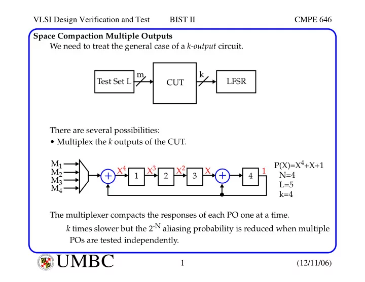
U M B C U N I V E R S I T Y O F M A R Y L A N D B A L T I M O R E C O U N T Y 1 9 6 6Space Compaction Multiple Outputs We need to treat the general case of a k-output circuit. There are several possibilities:
- Multiplex the k outputs of the CUT.
The multiplexer compacts the responses of each PO one at a time. k times slower but the 2-N aliasing probability is reduced when multiple POs are tested independently. Test Set L CUT m k LFSR
+
1
+
2 3 4 M1 M2 M3 M4 N=4 L=5 k=4 P(X)=X4+X+1 1 X X2 X3 X4