
SLIDE 1
Digital Systems Measurement Techniques I CMPE 650 1 (2/21/08)
UMBC
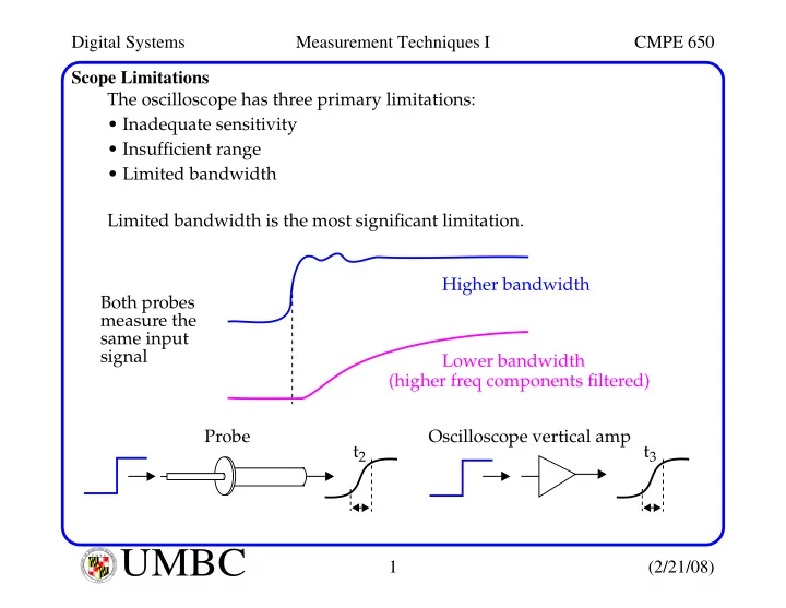
U M B C U N I V E R S I T Y O F M A R Y L A N D B A L T I M O R E C O U N T Y 1 9 6 6Scope Limitations The oscilloscope has three primary limitations:
- Inadequate sensitivity
- Insufficient range
- Limited bandwidth
Limited bandwidth is the most significant limitation. Higher bandwidth Lower bandwidth Both probes measure the same input signal (higher freq components filtered) Probe Oscilloscope vertical amp t2 t3