
SLIDE 1
Advanced VLSI Design Sequential Logic Design II CMPE 640 1 (12/6/04)
UMBC
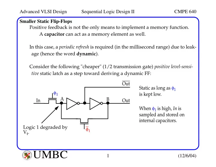
U M B C U N I V E R S I T Y O F M A R Y L A N D B A L T I M O R E C O U N T Y 1 9 6 6Smaller Static Flip-Flops Positive feedback is not the only means to implement a memory function. A capacitor can act as a memory element as well. In this case, a periodic refresh is required (in the millisecond range) due to leak- age (hence the word dynamic). Consider the following "cheaper" (1/2 transmission gate) positive level-sensi- tive static latch as a step toward deriving a dynamic FF: φ1 φ1 Out Static as long as φ1 is kept low. When φ1 is high, In is Out In sampled and stored on internal capacitors. A B Logic 1 degraded by Vt.