
SLIDE 1
Digital Systems Transmission Lines VII CMPE 650 1 (4/3/08)
UMBC
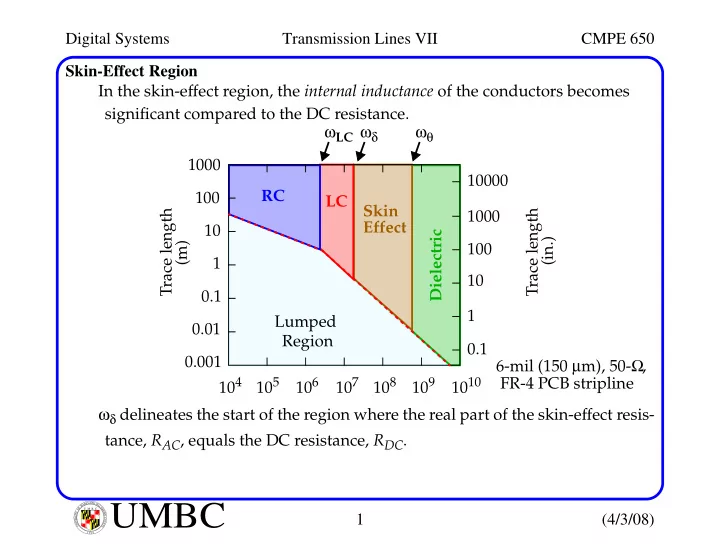
U M B C U N I V E R S I T Y O F M A R Y L A N D B A L T I M O R E C O U N T Y 1 9 6 6Skin-Effect Region In the skin-effect region, the internal inductance of the conductors becomes significant compared to the DC resistance. ωδ delineates the start of the region where the real part of the skin-effect resis- tance, RAC, equals the DC resistance, RDC. Region 0.001 0.01 0.1 1 10 100 1000 104 105 106 107 108 109 1010 Trace length (m) Trace length (in.) 0.1 1 10 100 1000 10000 RC ωLC LC Skin Effect Dielectric ωδ ωθ 6-mil (150 µm), 50-Ω, FR-4 PCB stripline Lumped