
SLIDE 1
Principles of VLSI Design Subsystem Design CMPE 413/CMSC 711 1 (December 11, 2000 3:44 pm)
UMBC
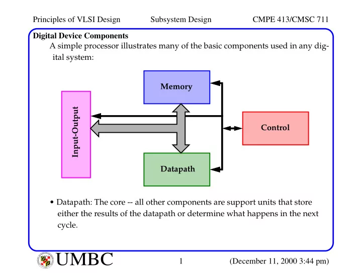
U M B C U N I V E R S I T Y O F M A R Y L A N D B A L T I M O R E C O U N T Y 1 9 6 6Digital Device Components A simple processor illustrates many of the basic components used in any dig- ital system:
- Datapath: The core -- all other components are support units that store
either the results of the datapath or determine what happens in the next cycle. Control Memory Datapath Input-Output