
SLIDE 1
Digital Systems Power, Speed and Packages II CMPE 650 1 (2/14/08)
UMBC
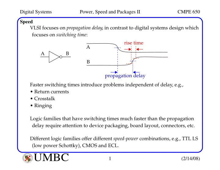
U M B C U N I V E R S I T Y O F M A R Y L A N D B A L T I M O R E C O U N T Y 1 9 6 6Speed VLSI focuses on propagation delay, in contrast to digital systems design which focuses on switching time: Faster switching times introduce problems independent of delay, e.g.,
- Return currents
- Crosstalk
- Ringing
Logic families that have switching times much faster than the propagation delay require attention to device packaging, board layout, connectors, etc. Different logic families offer different speed-power combinations, e.g., TTL LS (low power Schottky), CMOS and ECL. A B rise time propagation delay A B