
SLIDE 1
Systems Design & Programming Interrupts I CMPE 310 1 (April 24, 2002)
UMBC
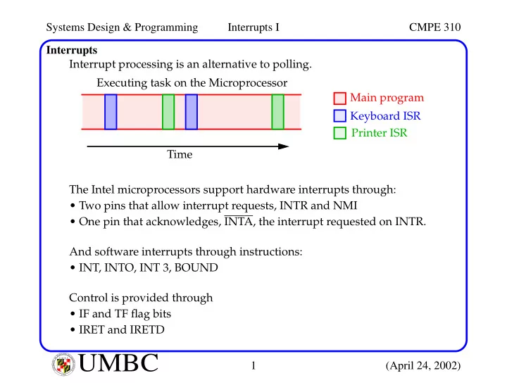
U M B C U N I V E R S I T Y O F M A R Y L A N D B A L T I M O R E C O U N T Y 1 9 6 6Interrupts Interrupt processing is an alternative to polling. The Intel microprocessors support hardware interrupts through:
- Two pins that allow interrupt requests, INTR and NMI
- One pin that acknowledges, INTA, the interrupt requested on INTR.
And software interrupts through instructions:
- INT, INTO, INT 3, BOUND
Control is provided through
- IF and TF flag bits
- IRET and IRETD
Time Executing task on the Microprocessor Main program Keyboard ISR Printer ISR