
Programmable Logic Devices Verilog Design Examples CMPE 415 1 (11/6/07)
UMBC
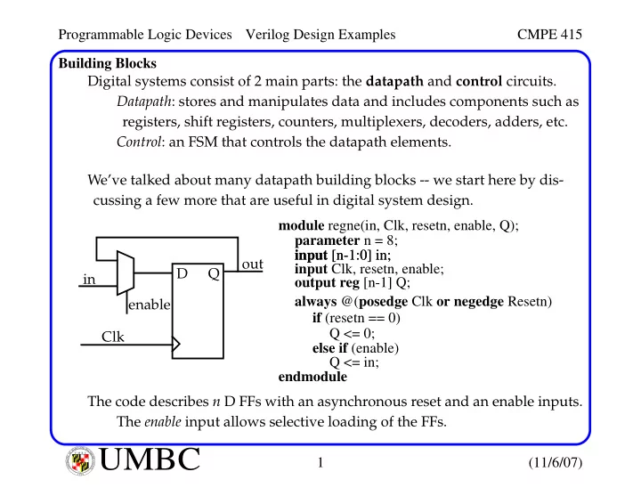
U M B C U N I V E R S I T Y O F M A R Y L A N D B A L T I M O R E C O U N T Y 1 9 6 6Building Blocks Digital systems consist of 2 main parts: the datapath and control circuits. Datapath: stores and manipulates data and includes components such as registers, shift registers, counters, multiplexers, decoders, adders, etc. Control: an FSM that controls the datapath elements. We’ve talked about many datapath building blocks -- we start here by dis- cussing a few more that are useful in digital system design. The code describes n D FFs with an asynchronous reset and an enable inputs. The enable input allows selective loading of the FFs. D Q in enable Clk
- ut
module regne(in, Clk, resetn, enable, Q); input [n-1:0] in;
- utput reg [n-1] Q;
always @(posedge Clk or negedge Resetn) if (resetn == 0) else if (enable) Q <= 0; Q <= in; parameter n = 8; input Clk, resetn, enable; input [n-1:0] in; endmodule