
SLIDE 1
VLSI Design Verification and Test Simulation CMPE 646 1 (11/26/07)
UMBC
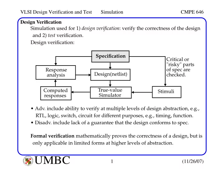
U M B C U N I V E R S I T Y O F M A R Y L A N D B A L T I M O R E C O U N T Y 1 9 6 6Design Verification Simulation used for 1) design verification: verify the correctness of the design and 2) test verification. Design verification:
- Adv. include ability to verify at multiple levels of design abstraction, e.g.,
RTL, logic, switch, circuit for different purposes, e.g., timing, function.
- Disadv. include lack of a guarantee that the design conforms to spec.
Formal verification mathematically proves the correctness of a design, but is
- nly applicable in limited forms at higher levels of abstraction.
Stimuli Specification True-value Response Design(netlist) Simulator analysis Computed responses Critical or "risky" parts
- f spec are
checked.