
SLIDE 1
Systems Design & Programming Memory III CMPE 310 1 (Mar. 6, 2002)
UMBC
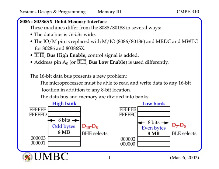
U M B C U N I V E R S I T Y O F M A R Y L A N D B A L T I M O R E C O U N T Y 1 9 6 68086 - 80386SX 16-bit Memory Interface These machines differ from the 8088/80188 in several ways:
- The data bus is 16-bits wide.
- The IO/M pin is replaced with M/IO (8086/80186) and MRDC and MWTC
for 80286 and 80386SX.
- BHE, Bus High Enable, control signal is added.
- Address pin A0 (or BLE, Bus Low Enable) is used differently.
The 16-bit data bus presents a new problem: The microprocessor must be able to read and write data to any 16-bit location in addition to any 8-bit location. The data bus and memory are divided into banks: FFFFFF FFFFFD 000003 000001 8 MB 8 bits D15-D8 FFFFFE FFFFFC 000002 000000 8 MB 8 bits D7-D0 High bank Low bank Odd bytes Even bytes BHE selects BLE selects