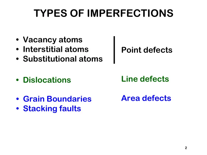
TYPES OF IMPERFECTIONS Vacancy atoms Interstitial atoms Point - - PowerPoint PPT Presentation

types of imperfections
SMART_READER_LITE
LIVE PREVIEW

TYPES OF IMPERFECTIONS Vacancy atoms Interstitial atoms Point - - PowerPoint PPT Presentation

TYPES OF IMPERFECTIONS Vacancy atoms Interstitial atoms Point defects Substitutional atoms Line defects Dislocations Area defects Grain Boundaries Stacking faults 2 No longer perfect: Thermal Energy Lattice


slide-1
SLIDE 1

2

  • Vacancy atoms
  • Interstitial atoms
  • Substitutional atoms
  • Dislocations
  • Grain Boundaries
  • Stacking faults

Point defects Line defects Area defects

TYPES OF IMPERFECTIONS

slide-2
SLIDE 2

No longer perfect: Thermal Energy

Lattice points Atom positions

Chapter 17 on CD

slide-3
SLIDE 3

8

  • Frenkel Defect
  • -a cation is out of place.
  • Shottky Defect
  • -a paired set of cation and anion vacancies.

Shottky Defect: Frenkel Defect

  • Equilibrium concentration of defects

~ e−QD /kT

Adapted from Fig. 13.20, Callister 5e. (Fig. 13.20 is from W.G. Moffatt, G.W. Pearsall, and J. Wulff, The Structure and Properties of Materials,

  • Vol. 1, Structure, John Wiley

and Sons, Inc., p. 78.) See Fig. 12.21, Callister 6e.

DEFECTS IN CERAMIC STRUCTURES

slide-4
SLIDE 4

Boltzmann's constant (1.38 x 10⁻²³ J/atom K) (8.62 x 10⁻⁵ eV/atom K)

⎜ ⎟ ND N = exp −QD kT ⎛ ⎝ ⎜ ⎞ ⎠ ⎟

  • No. of defects
  • No. of potential

defect sites. Activation energy Temperature Each lattice site is a potential vacancy site

4

  • Equilibrium concentration varies with temperature!
  • EQUIL. CONCENTRATION:

POINT DEFECTS

slide-5
SLIDE 5

5

  • We can get Q from

an experiment.

⎜ ⎟ ND N = exp −QD kT ⎛ ⎝ ⎜ ⎞ ⎠ ⎟

  • Measure this...
  • Replot it...

1/T N ND ln 1

  • QD/k

slope ND N T

exponential dependence!

defect concentration

MEASURING ACTIVATION ENERGY

slide-6
SLIDE 6

3

  • Vacancies:
  • vacant atomic sites in a structure.

Vacancy

distortion

  • f planes
  • Self-Interstitials:
  • "extra" atoms positioned between atomic sites.

self- interstitial

distortion

  • f planes

POINT DEFECTS

slide-7
SLIDE 7

9

Two outcomes if impurity (B) added to host (A):

  • Solid solution
  • f B

in A

(i.e., random dist. of point defects)

  • Solid solution of B

in A plus particles of a new phase (usually for a larger amount of B)

OR

Substitutional alloy (e.g., Cu in Ni) Interstitial alloy (e.g., C in Fe) Second phase particle

  • -different composition
  • -often different structure.

POINT DEFECTS IN ALLOYS

slide-8
SLIDE 8

11

  • Impurities must also satisfy charge balance
  • Ex: NaCl

Na+ Cl-

  • Substitutional cation impurity
  • Substitutional anion impurity

initial geometry Ca2+ impurity resulting geometry Ca2+ Na+ Na+ Ca2+

cation vacancy

initial geometry O2- impurity O2- Cl-

anion vacancy

Cl- resulting geometry

IMPURITIES

slide-9
SLIDE 9

13

  • are line defects,
  • cause slip between crystal plane when they move,
  • produce permanent (plastic) deformation.

Dislocations: Schematic of a Zinc (HCP):

  • before deformation
  • after tensile elongation

slip steps

LINE DEFECTS

slide-10
SLIDE 10

Edge dislocation

slide-11
SLIDE 11

15

  • Dislocations slip planes incrementally...
  • The dislocation line separates slipped material on the

left from unslipped material on the right. Dislocation motion requires the successive bumping

  • f a half plane of atoms (from left to right here).
  • Bonds across the slipping planes are broken and

remade in succession. Atomic view of edge dislocation motion from left to right as a crystal is sheared.

(Courtesy P.M. Anderson)

BOND BREAKING AND REMAKING

slide-12
SLIDE 12

Screw dislocation

slide-13
SLIDE 13

Area Defects

  • Surface
  • Grain boundary
slide-14
SLIDE 14

16

Grain boundaries:

  • are boundaries between crystals.
  • are produced by the solidification process, for example.
  • have a change in crystal orientation across them.
  • impede dislocation motion.

heat flow

Schematic

Adapted from Fig. 4.7, Callister 6e. Adapted from Fig. 4.10, Callister 6e. (Fig. 4.10 is from Metals Handbook, Vol. 9, 9th edition, Metallography and Microstructures, Am. Society for Metals, Metals Park, OH, 1985.)

~ 8cm

Metal Ingot

AREA DEFECTS: GRAIN BOUNDARIES

slide-15
SLIDE 15

Twin boundary

slide-16
SLIDE 16

17

  • Useful up to 2000X magnification.
  • Polishing removes surface features (e.g., scratches)
  • Etching changes reflectance, depending on crystal
  • rientation.

microscope

close-packed planes micrograph of Brass (Cu and Zn)

Adapted from Fig. 4.11(b) and (c), Callister 6e. (Fig. 4.11(c) is courtesy

  • f J.E. Burke, General Electric Co.

0.75mm

OPTICAL MICROSCOPY (1)

slide-17
SLIDE 17

Fe-Cr alloy

microscope grain boundary surface groove polished surface

18

Grain boundaries...

  • are imperfections,
  • are more susceptible

to etching,

  • may be revealed as

dark lines,

  • change direction in a

polycrystal.

Adapted from Fig. 4.12(a) and (b), Callister 6e. (Fig. 4.12(b) is courtesy

  • f L.C. Smith and C.

Brady, the National Bureau of Standards, Washington, DC [now the National Institute of Standards and Technology, Gaithersburg, MD].)

ASTM grain size number

N = 2n-1

  • no. grains/in2

at 100x magnification

OPTICAL MICROSCOPY (2)

slide-18
SLIDE 18

20

  • Point, Line, and Area

defects arise in solids.

  • The number and type of defects can be varied

and controlled (e.g., T controls vacancy conc.)

  • Defects affect material properties (e.g., grain

boundaries control crystal slip).

  • Defects may be desirable or undesirable

(e.g., dislocations may be good or bad, depending

  • n whether plastic deformation is desirable or not.)

SUMMARY