
SLIDE 1
A.E. Gunnæs MENA3100 V18
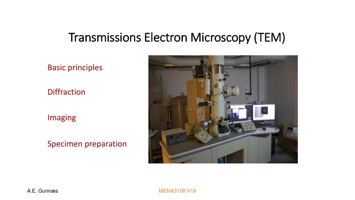
Transmissions Ele lectron Mic icroscopy (T (TEM) Basic principles - - PowerPoint PPT Presentation
Transmissions Ele lectron Mic icroscopy (T (TEM) Basic principles Diffraction Imaging Specimen preparation A.E. Gunns MENA3100 V18 Electron interaction with the (thin) specimen e - Typical specimen thickness Backscattered electrons ~
A.E. Gunnæs MENA3100 V18
Specimen
Transmitted electrons Inelastically scattered electrons X-rays Secondary electrons Backscattered electrons Auger electrons Cathodoluminescence Gas Heating Cooling Absorbed electrons EBIC Elastically scattered electrons Typical specimen thickness ~ 100 nm or less
Electrons interacts 100-1000 times stronger with matter than X-rays
Convergent beam Parallel beam
Can be scanned (STEM mode)
Specimen
Spectroscopy and mapping (EDS and EELS)
Quartz (1mm) AZO (sputtering, ~200 nm) Cu2O (sputtering, 600nm) TiO2 (ALD, 10 nm)
Example of EDS mapping in STEM mode.
EDS: Energy dispersive spectroscopy EELS: Electron energy loss spectroscopy STEM: Scanning transmission electron microscopy HAADF: High angular annular dark field
With spatial resolution down to the atomic level (HREM and STEM) Chemistry and elecronic states (EDS and EELS). Spatial and energy resolution down to the atomic level and ~0.1 eV. From regions down to a few nm (CBED).
200 nm
HREM: High resolution electron microscopy BF: Bright field CBED: Convergent beam electron diffraction SAD: Selected area diffraction
SAD pattern BF TEM image
A.E. Gunnæs
Resolution of the eyes:~ 0.1-0.2 mm Resolution in a visible light microscope: ~200 nm
Defects Precipitates Interfaces
Important for material properties
CuO ZnO
HAADF image Strain analysis around a dislocation core at the CuO-ZnO interface
Local atomic structure and composition, Electronic structure and chemical bonding
A.E. Gunnæs
Goal to produce single phase:
BiFeO3 with space grupe: R3C and celle dimentions: a= 5.588 Å c=13.867 Å Metal organic compound on Pt Heat treatment at 350oC (10 min) to remove organic parts. Process repeated three times before final heat treatment at 500-700 oC (20 min) . (intermetallic phase grown)
BF TEM image of the cross section of the specimen 200 nm Si SiO2 TiO2 Pt BiFeO3 Lim Glue A.E. Gunnæs
50 nm Tilting series around a dens row of reflections in the reciprocal space 0o 19o 25o 40o 52o
Courtesy: Dr. Jürgen Thomas, IFW-Dresden, Germany
Positions of the reflections in the reciprocal space
Elastic scattered electrons
Only the direction of v is changing. (Bragg scattering) Elastic scattering is due to Coulomb interaction between the incident electrons and the electric charge of the electron clouds and the nucleus. (Rutherford scattering). The elastic scattering is due to the average position of the atoms in the lattice. Reflections satisfying Braggs law:
2dsinθ=nλ
Electrons interacts 100-1000 times stronger with matter than X-rays
Courtesy: Dr. Jürgen Thomas, IFW-Dresden, Germany
From the tilt series we find that the unknown phase has a primitive orthorhombic Bravias-lattice with cell parameters: a= 6,04 Å, b= 7.94 Å og c=8.66 Å α= β= γ= 90o
6.04 Å 7.94 Å
a b c 100 110 111 010 011 001 101 [011] [100] [101] d = L λ / R
Ukjent fase BiFeO3 BiFe2O5
10 15 20 25 30 35 40 Nr_2_1evprc.PICT
200 400 600 800 1000
2 4 6 8 10 12 14 Energy Loss (eV) CCD counts x 1000
Ukjent fase BiFeO3 Fe - L2,3 O - K 500 eV forskyvning, 1 eV pr. kanal
A.G. Tutov og V.N. Markin The x-ray structural analysis of the antiferromagnetic Bi2Fe4O9 and the isotypical combinations Bi2Ga4O9 and Bi2Al4O9 Izvestiya Akademii Nauk SSSR, Neorganicheskie Materialy (1970), 6, 2014-2017. Romgruppe: Pbam nr. 55, celleparametre: 7,94 Å, 8,44 Å, 6.01Å x y z Bi 4g 0,176 0,175 Fe 4h 0,349 0,333 0,5 Fe 4f 0,5 0,244 O 4g 0,14 0,435 O 8i 0,385 0,207 0,242 O 4h 0,133 0,427 0,5 O 2b 0,5
O Bi Fe O Fe Bi O Fe O O O Fe Fe O O O O Fe Bi O O Bi O Bi O O Bi Fe O O O O Fe Fe O O O Fe O Bi Fe O Fe Bi O PCelle parameters found with electron diffraction (a= 6,04 Å, b= 7.94 Å and c=8.66 Å) fits reasonably well with the previously published data for the Bi2Fe4O9 phase. The disagreement in the c-axis may be due to the fact that we have been studying a thin film grown on a crystalline substrate and is not a bulk sample. The conditions for reflections from the space group Pbam is in agreement with observations done with electron diffraction. Conclusion: The unknown phase has been identified as Bi2Fe4O9 with space group Pbam with cell parameters a= 6,04 Å, b= 7.94 Å and c=8.66 Å.
A.E. Gunnæs
A.E. Gunnæs
Electron gun Apertures Sample holder Fluorescence screen Recording media (Cameras, detectors)
Vacuum in the column better than 10-6 Pa
Sample
condenser lenses Objective lens Intermediate lenses Projector lens
Similar components as a transmission light microscope
W ZrO/W
Cold FEG Schottky FEG
Thermionic emission
Filament heated to give thermionic emission
indirectly (LaB6)
Filament negative potential to ground Wehnelt produces a small negative bias
cross over
considerably increased at sharp points.
that electrons can tunnel out of the tungsten.
if tip is heated (”thermal” FE; ZrO surface tratments → Schottky emitters).
(JEOL2100F: 0.19 nm)
The point resolution in a TEM is limited by the aberrations of the lenses.
A charged particle such as an electron, is deflected by a magnetic field. The direction and magnitude of the force F,
Electron gun Apertures Sample holder Fluorescence screen Recording media (Cameras, detectors)
Vacuum in the column better than 10-6 Pa
Sample
condenser lenses Objective lens Intermediate lenses Projector lens
Similar components as a transmission light microscope
Simplified ray diagram
Objective lense Diffraction plane (back focal plane) Image plane Sample Parallel incoming electron beam Si
1,1 nm 3,8 Å
Objective aperture Selected area aperture
Objective lense Diffraction pattern Image plane Specimen with two crystals (red and blue)
Parallel incoming electron beam
Selected area aperture
Pattern on the screen
polycrystalline sample if the aperture is small enough/crystal large enough.
– XRD is much more accurate
Poly crystalline sample
The orientation relationship between the phases can be determined with ED.
25 Single Crystals Interface between two different phases epitaxially grown
Amorphous phase
Similarities to XRD
Courtesy: Dr. Jürgen Thomas, IFW- Dresden, Germany
Cu Kalpha X-ray: = 150 pm => small k
The radius of the Ewald sphere is 1/ (=k) Resiprocal lattice of a crystal ko k
Electrons at 200 kV: = 2.5 pm => large k
The dimensions of the specimen affects the shape of the resiprocal lattice poins
2d sinθ = nλ
λ200kV = 0.00251 nm Θ~1o I(k’-k)I=(2/λ)sinθB=g
Zone axis [uvw] (hkl)
uh+vk+wl= 0
The g vector to a reflection is normal to the corresponding (h k l) plane and IgI=1/dnh nk nl
the reflections
calculated d-values of possible phases
cubic structure.
(h2k2l2) Orientations of corresponding planes in the real space
A.E. Gunnæs
200 nm Si SiO2 TiO2 Pt BiFeO3 Glue
1 1 1 2
The eyes can not see intensity chanes that is less then 5-10%, however, contrast in images can be enhanced digitally. NB! It is correct to talk about strong and week contrast but not bright and dark contrast
Condenser aperture:
Limits the number of electrons reaching the specimen (reducing the intensity), Affecting the convergent of the electron beam.
Selected area aperture:
Allows only electrons going through an area on the sample that is limited by the SAD aperture to contribute to the diffraction pattern (SAD pattern).
Objective aperture:
Allows certain reflections to contribute to the image. Increases the contrast in the image. Bright field imaging (central beam, 000), Dark field imaging (one reflection, g), High resolution Images (several reflections from a zone axis).
Simplified ray diagram
Objective lense Diffraction plane (back focal plane) Image plane Sample Parallel incoming electron beam Si
1,1 nm 3,8 Å
Objective aperture Selected area aperture
A.E. Gunnæs
No aperture used Central beam selected Si Ag and Pb glue
(light elements)
hole
TEM variables that affect the contrast:
Areas of greater Z and/or t scatter electrons more strongly (in total).
Incoherent elastic scattering (Rutherford scattering): peaked in the forward direction, t and Z-dependent
Williams and Carter, TEM, Part 3 Springer 2009
A.E. Gunnæs
50 nm
Try to make an illustration to explain why we get this enhanced contrast when only the central beam is selected by the optical aperture.
A.E. Gunnæs Bright field image
Brigh right field field (BF (BF), d dark rk field field (DF (DF) and Hig High res esolu lution EM (HR (HREM)
BF image Objective aperture DF image
HREM image
http://www.mathematik.com/Moire/ A Moiré pattern is an interference pattern created, for example, when two grids are overlaid at an angle, or when they have slightly different mesh sizes (rotational and parallel Moire’ patterns). HREM image
Long-Wei Yin et al., Materials Letters, 52, p.187-191
Interference pattern
A.E. Gunnæs MENA3100 V18
A.E. Gunnæs
Specimen
TEM mode with parallel incoming electron beam Change the strength
The diffraction pattern or image of the specimen is magnified
Specimen
TEM mode with parallel incoming electron beam Apertures
(No: Blendere)
Condenser Object SAD SAD aperture: used to select an area on the specimen one want diffraction date from (on the second intermediat image and projected).
Specimen
TEM mode with parallel incoming electron beam Apertures
(No: Blendere)
Condenser Object SAD Objective aperture: used to select which electron beams will contribute to the image (on the second intermediat image and projected).
TEM mode with parallel incoming electron beam Objective aperture: used to select which electron beams will contribute to the image (on the second intermediat image and projected). The objective aperture is used to controls the contrast in the image (enhances contrast). One beam: Amplitude contrast (central (BF) or a scattered beam (DF)) Two or more beams: Phase contrast (+ amplitude) (HREM images (zone axis) or Moire)
Brigh right field field (BF (BF), d dark rk field field (DF (DF) and Hig High res esolu lution EM (HR (HREM)
BF image Objective aperture DF image
HREM image
A TEM image will in most cases show both contrast types
TEM variables that affect the contrast:
Areas of greater Z and/or t scatter electrons more strongly (in total).
Incoherent elastic scattering (Rutherford scattering): peaked in the forward direction, t and Z-dependent
Williams and Carter, TEM, Part 3 Springer 2009
A.E. Gunnæs Bright field image
50 nm The contrast is very sencitive to the specimen orientation. (In contrast to mass-density contrast)
200 nm Si SiO2 TiO2 Pt BiFeO3 Glue
A.E. Gunnæs
BF image DF image DF image
sample
Solberg, Jan Ketil & Hansen, Vidar (2001). Innføring i transmisjon elektronmikroskopi
in the diffracted intensity with increasing thickness of the sample
intensities
Incident beam Diffracted beam Doubly diffracted beam Transmitted beam Wedge shaped TEM sample t0
Basis of kinematical theory of electron diffraction for imperfect crystals: Ψg(t)= ∫(πi/ξg) exp(-2πisgz)dz, Ψo=1, t: crystal thickess
t
Intensity of the scattered beam g (dark field): Ig= l Ψg(t) l2= sin2 πsgt/(ξgsg)2 Intensity of the unscattered beam 0 (bright field): I0= 1-Ig= 1- l Ψg(t) l2= 1 - sin2 πsgt/(ξgsg)2 Ψg(t)= (i/ξgsg) exp(-πitsg) sinπsgt
A.E. Gunnæs MENA3100 V10
Sample (side view) e 000 g t Ig=1- Io In the two-beam situation the intensity
is periodic with thickness (Ig=1- Io) Sample (top view) Hole Positions with max Intensity in Ig
Intensity of the scattered beam g: Ig= l Ψg(t) l2= sin2 πsgt/(ξgsg)2
A.E. Gunnæs MENA3100 V10
Sample Sample DF image BF image
Zone axis pattern Need to have a thick specimen region Close to a zone axis
scattered electrons falls of rapidly with angle. I=Iocos2α
http://www.doitpoms.ac.uk/index.html http://www.doitpoms.ac.uk/tlplib/diffraction-patterns/kikuchi.php
Excess Deficient Excess line Deficient line
2θB θB θB
Diffraction plane Objective lens
1/d
. 1.Ineleastic scattering +
Incoherently and inelastically (ΔE~15-25 eV) scattered electrons give rise to diffuse background in the ED pattern
http://www.umsl.edu/~fraundorfp/nanowrld/live3Dmodels/vmapframe.htm 000 g
Ig=I-g Sg<0 Sg=0 Effect of tilting the specimen Kossel cones Parabolas g and –g Kikuchi lines
ultramicrotomy
3 mm
A.E. Gunnæs Grind down/ dimple
in film films
Cut out a cylinder and glue it in a Cu-tube Grind down and glue on support rings Cut a slice of the cylinder and grind it down / dimple
Ione beam thinning
Cut out cylinder
Ione beam thinning
Cut out slices Glue the interface
face together with support material Cut off excess material
(FIB)