
SLIDE 1
10 June 2010
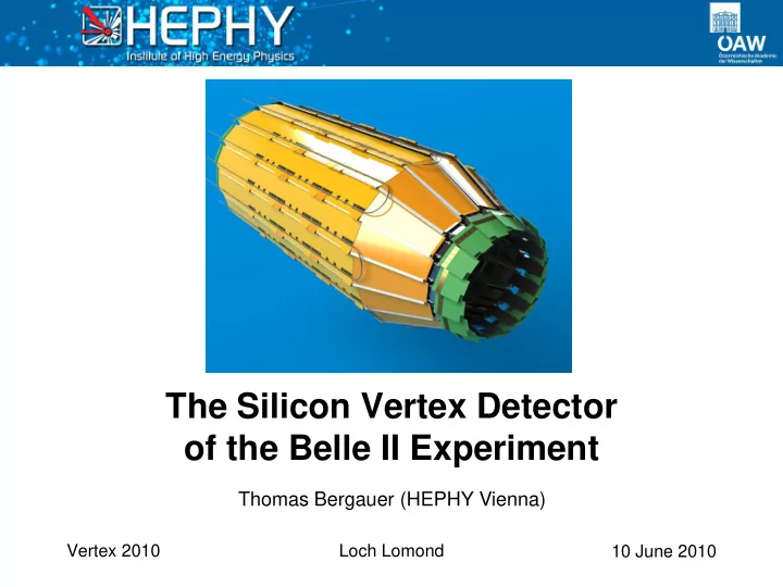
The Silicon Vertex Detector
- f the Belle II Experiment
Vertex 2010
Thomas Bergauer (HEPHY Vienna)
Loch Lomond
The Silicon Vertex Detector of the Belle II Experiment Thomas - - PowerPoint PPT Presentation
The Silicon Vertex Detector of the Belle II Experiment Thomas Bergauer (HEPHY Vienna) Vertex 2010 Loch Lomond 10 June 2010 The Silicon Vertex Detector of the Belle II Experiment Introduction Belle II: The Future Double Sided Sensors
10 June 2010
Vertex 2010
Loch Lomond
10 June 2010
2
10 June 2010
~1 km in diameter
3
10 June 2010
4
10 June 2010
5
10 June 2010
6
10 June 2010
7
10 June 2010
8
10%
10 June 2010
10 1 2 3 4 [cm] layers [cm] 20
10 20 30 40
9
10 June 2010
10 1+2 3 4 5 6 [cm] layers [cm] 20
10 20 30 40
10
10 June 2010
11
10 June 2010
12
13 Thomas Bergauer (HEPHY Vienna)
6 6 4 4 4 4 4 6 6 6 6 6 4 4 4 4 4 4 4 6 6 6 6 6 6 6 6 6
10 June 2010 14
15
10 June 2010
10 June 2010
Trapezoidal sensor with test structures
17
Sensor “programming language”
10 June 2010
18
10 June 2010
Schematics of one channel
19
10 June 2010
50 100 150 200 250 300
5000 10000 15000 20000 25000 30000
S peak tpeak
20
Threshold Threshold Tim e over threshold ~ 2000ns (m easured) Tim e over threshold ~ 160ns (m easured) Sensitive tim e window ~ 20ns
VA 1TA
Tp~800ns
APV25
Tp~50ns Pulse shape processing RM S(tm ax)~3ns
10 June 2010 21
10 June 2010
zylon rib APV25 cooling pipe 3-layer kapton hybrid integrated fanout DSSD double-layer flex wrapped to p-side
APV25 (thinned to 100µm ) zylon rib cooling pipe DSSD Rohacell Kapton
22
10 June 2010 23
23
– Currently under test in Vienna
24
10 June 2010
10 June 2010
25
10 June 2010
26
10 June 2010
27
10 June 2010
1902 APV25 chips Front-end hybrids Rad-hard voltage regulators Analog level translation, data sparsification and hit time reconstruction Unified Belle II DAQ system ~2m copper cable Junction box ~10m copper cable FADC+PROC COPPER Unified optical data link (>20m) Finesse Transmitter Board (FTB) 28
10 June 2010
29
10 June 2010
30
10 June 2010
31
10 June 2010
32
10 June 2010 33
y * (mm)
x (nm)
y( m)
y
z (mm)
35
10 June 2010 Crab cavity 3.5GeV e 8GeV e New beam-pipes with ante-chamber Damping ring for e+ New IR with crab crossing and smaller y* More RF for higher beam current SR beam
10 June 2010 36
37 Thomas Bergauer (HEPHY Vienna)
Teststructures for p-side Teststructures for n-side (no GCD) Baby sensor 1 p-side: 512 strips 50 µm pitch 1 interm. strip n-side: 512 strips 100 µm pitch 1 interm. strip atoll p-stop 3 different GCDs for the n-side Main sensor p-side: 768 strips 75-50 µm pitch 1 interm. strip n-side: 512 strips 240 µm pitch 1 interm. strip combined p-stop Quadratic baby sensors 2,3,4 p-side: 512 strips 50 µm pitch 1 interm. strip n-side: 256 strips 100 µm pitch 0 interm. strip different p-stop patterns 1) atoll p-stop varying distance from strip 2) conventional p-stop varying width 3) combined p-stop varying distance from strip 1) 2) 3)
38 Thomas Bergauer (HEPHY Vienna)
Slanted Sensors Origami Cooling Tubes Hybrid Boards
Layer Sensors/ Ladder Origamis/ Ladder Ladders Length [mm] Radius [mm] Slant Angle [°]
3 2 7/8 262 38 4 3 1 10 390 80 11.9 5 4 2 14 515 115 17.2 6 5 3 17 645 140 21.1
10 June 2010 39
10 June 2010 40
10 June 2010
T im e Resolution vs. C luster S NR 1 2 3 4 5 6 7 5 10 15 20 25 30 C luster S NR [1] trm s [ns] P revious beam tests S P S 09 beam test Log-Log Fit
(TDC error subtracted) Origami Module
41
Conventional (double layer kapton)
Layer M aterial X0 [m m ] Thickness [m m ] Percentage Area coverage Averaged Percentage Sensor Silicon 93.7 0.3 0.32% 100.0% 0.320% Fanout Polyim ide (2 layer of 50um each) 300.0 0.1 0.03% 96.3% 0.032% Copper (10um ) 14.0 0.01 0.07% 50.0% 0.036% Nickel (top: 1.3um ) 14.3 0.0013 0.01% 50.0% 0.005% G old (top: 0.8um ) 3.4 0.0008 0.02% 50.0% 0.012% Ribs Zylon (0.5m m wide) 300.0 5 1.67% 3.7% 0.062% G lue Araldite 2011 / Double sided tape 335.0 0.05 0.01% 96.3% 0.014%
Total 0.480% DSSD Chip-on-Sensor (4-layer kapton)
Layer M aterial X0 [m m ] Thickness [m m ] Percentage Area coverage Averaged Percentage Sensor Silicon 93.7 0.3 0.32% 100.0% 0.320% Isolation Rohacell (Degussa) 5450.0 1 0.02% 96.3% 0.018% Hybrid Polyim ide (4 layers of 50um each) 300.0 0.2 0.07% 96.3% 0.064% Copper (4 layers of 5um each) 14.0 0.02 0.14% 64.7% 0.092% Nickel (top: 1.3um ) 14.3 0.0013 0.01% 64.7% 0.006% Flash Gold (top: 0.4um ) 3.4 0.0004 0.01% 64.7% 0.008% Flexes Polyim ide (1 layer of 25um ) 300.0 0.025 0.01% 56.3% 0.005% Copper (1 layer of 5um ) 14.0 0.005 0.04% 28.1% 0.010% Nickel (top: 1.3um ) 14.3 0.0013 0.01% 28.1% 0.003% Flash Gold (top: 0.4um ) 3.4 0.0004 0.01% 28.1% 0.003% 8 * APV25 Silicon 93.7 0.1 0.11% 21.4% 0.023% SM Ds SM D 50.0 0.4 0.80% 0.8% 0.007% Sil-Pad Sil-Pad 800 (Bergquist) 200.0 0.127 0.06% 11% 0.007% Pipe Alum inum (D=2.0m m , wall=0.2m m ) 89.0 0.56 0.63% 7% 0.047% Rib Zylon (0.5m m wide) 300.0 5 1.67% 1.9% 0.031% Glue Araldite 2011 335.0 0.2 0.06% 50% 0.030% Cooling W ater 360.5 1.26 0.35% 13% 0.047%
Total 0.719%
10 June 2010 42
10 20 30 40 50 60 0.5 1 1.5 2 2.5 3 3.5 Profile [mm] R adiation Length [%] R ib Design
10 June 2010 43
Origamis/ Ladder Ladders APVs Origami APVs Hybrid Layer 6 3 17 510 340 Layer 5 2 14 280 280 Layer 4 1 10 100 200 Layer 3 8 192
10 June 2010 44