technology impact horizon
play

Technology impact horizon In order of earliest to - PowerPoint PPT Presentation

Technology impact horizon In order of earliest to market probability: Secure quantum networks for communica2ons Quantum sensing that does not


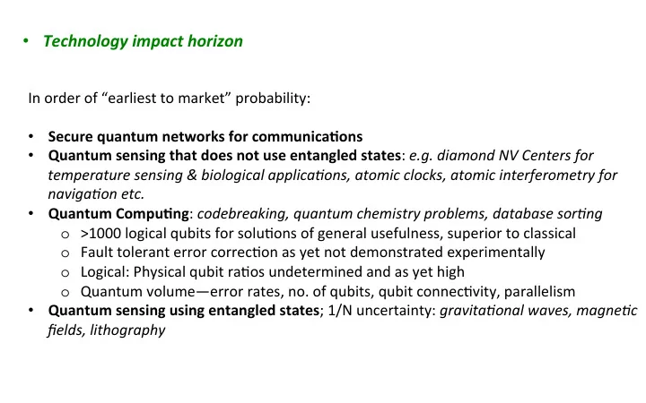
  1. • Technology ¡impact ¡horizon ¡ In ¡order ¡of ¡“earliest ¡to ¡market” ¡probability: ¡ ¡ • Secure ¡quantum ¡networks ¡for ¡communica2ons ¡ • Quantum ¡sensing ¡that ¡does ¡not ¡use ¡entangled ¡states : ¡ e.g. ¡diamond ¡NV ¡Centers ¡for ¡ temperature ¡sensing ¡& ¡biological ¡applica8ons, ¡atomic ¡clocks, ¡atomic ¡interferometry ¡for ¡ naviga8on ¡etc. ¡ • Quantum ¡Compu2ng : ¡ codebreaking, ¡quantum ¡chemistry ¡problems, ¡database ¡sor8ng ¡ o >1000 ¡logical ¡qubits ¡for ¡solu=ons ¡of ¡general ¡usefulness, ¡superior ¡to ¡classical ¡ o Fault ¡tolerant ¡error ¡correc=on ¡as ¡yet ¡not ¡demonstrated ¡experimentally ¡ o Logical: ¡Physical ¡qubit ¡ra=os ¡undetermined ¡and ¡as ¡yet ¡high ¡ o Quantum ¡volume—error ¡rates, ¡no. ¡of ¡qubits, ¡qubit ¡connec=vity, ¡parallelism ¡ • Quantum ¡sensing ¡using ¡entangled ¡states ; ¡1/N ¡uncertainty: ¡ gravita8onal ¡waves, ¡magne8c ¡ fields, ¡lithography ¡ ¡

  2. Quantum ¡Informa2on ¡Systems: ¡scalable, ¡pa?ernable ¡solid ¡state ¡systems ¡ solid state single photon quantum quantum sources/detectors memory qubits transducers single ¡photon ¡source& ¡detector ¡ programmable ¡ quantum ¡memory ¡ processor ¡ transducer ¡ transducer ¡ programmable ¡ repeater ¡ processor ¡ programmable ¡ op=cal ¡link ¡ q. ¡sensor ¡ processor ¡ ¡Chicago ¡Quantum ¡Exchange ¡ ¡

  3. Major ¡materials ¡and ¡process ¡challenges ¡ ¡ • Unlike ¡Si ¡CMOS: ¡quantum ¡processor ¡system ¡size ¡(# ¡of ¡devices) ¡is ¡controlled ¡by ¡qubit ¡error ¡rates ¡and ¡not ¡litho ¡scaling. ¡ • Very ¡likely ¡solid ¡state ¡coherent ¡systems ¡will ¡be ¡integrated ¡with ¡silicon ¡at ¡different ¡in=macies— ¡ • Needs ¡are ¡broadly ¡compa=ble ¡with ¡exisi=ng ¡process ¡infrastructure ¡(with ¡some ¡excep=ons) ¡ ¡ Challenges: ¡ 1) Miniaturiza=on ¡of ¡devices: ¡Bulk ¡to ¡nanoscale ¡sizing ¡ 2) New ¡materials ¡discovery ¡and ¡integra=on ¡with ¡silicon ¡tech. ¡ o Stability ¡(such ¡as ¡coherence ¡=me) ¡& ¡variability ¡(such ¡as ¡frequency) ¡are ¡key—materials ¡response ¡not ¡well ¡ understood, ¡ o Master ¡difficult ¡to ¡process ¡and ¡integrate ¡material—tough ¡oxides ¡e.g. ¡ o Manipula=on ¡of ¡quantum ¡devices: ¡nanophotonics ¡becomes ¡increasingly ¡important ¡ 3) Atom ¡scale ¡nanofabrica=on—move ¡away ¡from ¡non-­‑determinis=c ¡processing ¡ ¡Chicago ¡Quantum ¡Exchange ¡ ¡

  4. #1: ¡Miniaturiza2on ¡of ¡devices; ¡example ¡of ¡the ¡transducer ¡ (Xufeng ¡Zhang, ¡Argonne) ¡ Transistor ¡ µ wave ¡ 1947 ¡ magnon ¡ op=cal ¡ photon ¡ photon ¡ Today ¡ Superconduc=n Quantum ¡ YIG ¡transducer ¡ g ¡qubit ¡ photonics ¡ Quantum ¡transducer ¡ Photonic ¡circuits ¡ S.C ¡circuits ¡ YIG ¡sphere ¡ Today ¡ -10 Magnitude (dB) -15 RF ¡port ¡ ? ¡ 500 ¡um ¡ 11.0 11.2 11.4 Frequency (GHz) ¡Chicago ¡Quantum ¡Exchange ¡ ¡

  5. New ¡materials ¡discovery ¡and ¡integra=on ¡with ¡silicon ¡tech……one ¡more ¡example ¡ 2) ¡Oxides ¡for ¡solid ¡state ¡coherent ¡quantum ¡memory ¡ ¡ • Implemen=ng ¡a ¡long ¡channel ¡ • Divide ¡the ¡channel ¡into ¡sec=ons ¡connected ¡by ¡ quantum ¡repeaters ¡ • Quantum ¡memories ¡are ¡central ¡to ¡these ¡repeaters ¡ • Large ¡field ¡of ¡viable ¡candidates ¡ • NV ¡centers, ¡defects ¡in ¡SiC, ¡divacancies ¡in ¡Si/Ge, ¡rare ¡earth ¡ions ¡(REI) ¡etc. ¡ ¡Chicago ¡Quantum ¡Exchange ¡ ¡

  6. 2) ¡A ¡scalable, ¡oxide ¡thin ¡film ¡plaMorm ¡for ¡storing ¡light ¡qubits ¡ Defect ¡type ¡ Coherence ¡ Coherence ¡ Retrieval ¡ Retrieval ¡ 2me ¡(at ¡mK) ¡ 2me ¡(at ¡RT) ¡ Efficiency ¡ Fidelity ¡ NV ¡in ¡Diamond ¡ > ¡1 ¡sec ¡ ¡ > ¡100 ¡us ¡ > ¡75% ¡ 0.85 ¡ SiV ¡in ¡Diamond ¡ > ¡10 ¡ms ¡ NA ¡ -­‑ ¡ SiC ¡di-­‑vacancies ¡ > ¡1 ¡ms ¡ NA ¡ -­‑ ¡ Rare ¡earth ¡ions ¡ Eu ¡in ¡YSO ¡ > ¡6 ¡hours ¡ NA ¡ NA ¡ -­‑ ¡ Er ¡in ¡YSO ¡ >1.3 ¡sec ¡ NA ¡ >50% ¡ 0.93 ¡ • Er 3+ ¡op=cal ¡transi=on ¡lies ¡in ¡the ¡telecom ¡C ¡band ¡ • Ynria ¡(Y 2 O 3 ) ¡is ¡a ¡low ¡noise ¡host ¡material ¡ ¡ • Y 2 O 3 ¡thin ¡films ¡can ¡be ¡grown ¡epitaxially ¡on ¡Si ¡ • Lithography ¡can ¡be ¡used ¡for ¡at ¡scale ¡device ¡development ¡ ¡ ¡Chicago ¡Quantum ¡Exchange ¡ ¡ [1] ¡ Guha , ¡ Appl. ¡Phys. ¡Len. ¡80, ¡766 ¡(2002) ¡ ¡

  7. Coupling ¡to ¡nanophotonic ¡structures ¡for ¡quantum ¡memories ¡ Epitaxial ¡growth ¡of ¡high ¡ quality ¡rare-­‑earth ¡thin ¡ films ¡on ¡Si ¡ tapered ¡ fiber ¡laser ¡ coupling ¡ Qualify ¡ ¡Er:Y 2 O 3 ¡as ¡a ¡ quantum ¡memory ¡ Op=cal ¡& ¡Spin ¡T 1 ¡and ¡T 2 ¡ b) ¡ a) ¡ measurements ¡ O Y 2 O 3 ¡ Y Demonstra=on ¡of ¡a ¡ working ¡quantum ¡ Si-­‑Y 2 O 3 ¡ b ¡ a ¡ a ¡ b ¡ memory ¡ SiO x ¡ Si ¡substrate ¡ [001] ¡ ¡Chicago ¡Quantum ¡Exchange ¡ ¡

  8. CHICAGO QUANTUM EXCHANGE § A Growing Intellectual Hub for the Science and Engineering of Quantum Information Science Launching a communications testbed • teleportation link 30 miles of single-mode telecom fiber • encryption testbed

Download Presentation
Download Policy: The content available on the website is offered to you 'AS IS' for your personal information and use only. It cannot be commercialized, licensed, or distributed on other websites without prior consent from the author. To download a presentation, simply click this link. If you encounter any difficulties during the download process, it's possible that the publisher has removed the file from their server.

Recommend


More recommend