
SLIDE 1
Synthesis Script for 8 x 8 Binary Multiplier
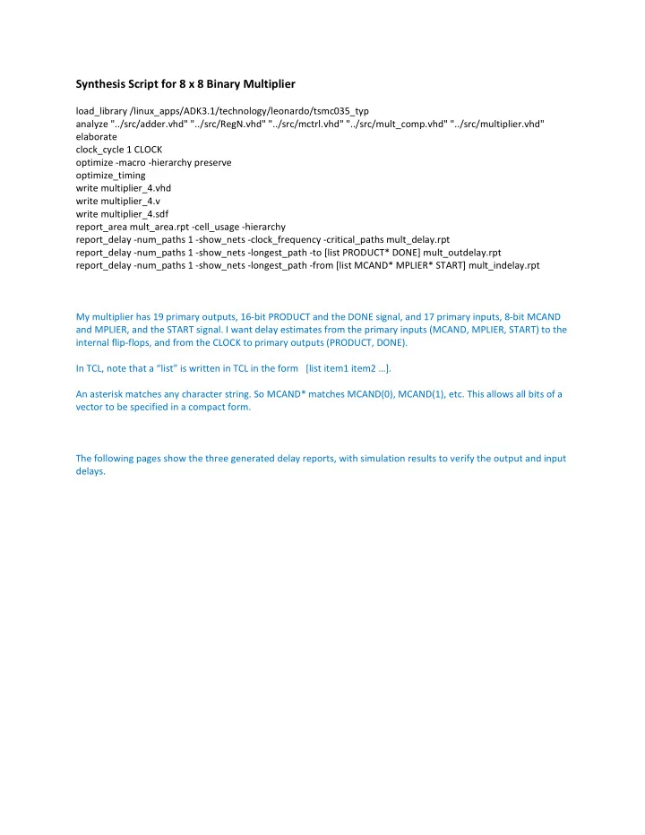
load_library /linux_apps/ADK3.1/technology/leonardo/tsmc035_typ analyze "../src/adder.vhd" "../src/RegN.vhd" "../src/mctrl.vhd" "../src/mult_comp.vhd" "../src/multiplier.vhd" elaborate clock_cycle 1 CLOCK
- ptimize -macro -hierarchy preserve
- ptimize_timing