
SLIDE 1
Semicond emiconductor uctor Nano-S Nano-Spintro pintronics nics
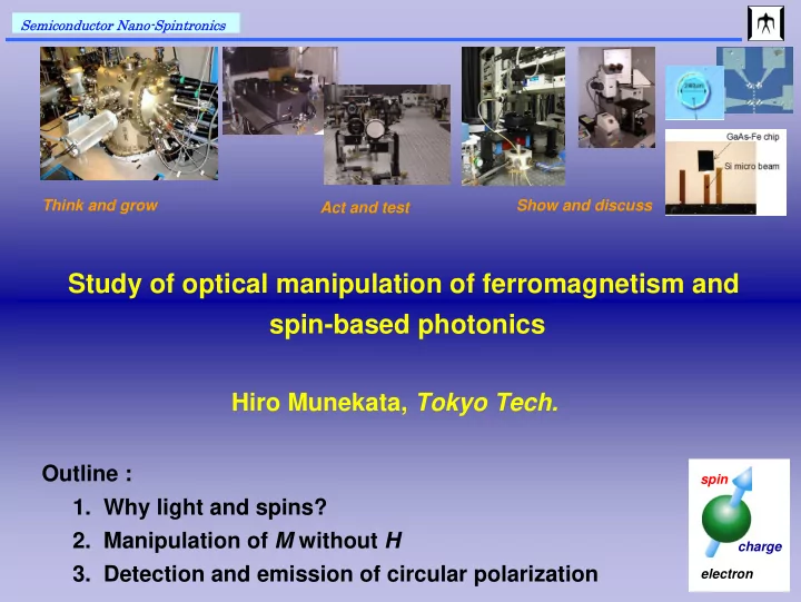
Think and grow Act and test Show and discuss
Outline :
- 1. Why light and spins?
- 2. Manipulation of M without H
- 3. Detection and emission of circular polarization
spin electron charge