strucuture and photoluminescence properties
play

STRUCUTURE AND PHOTOLUMINESCENCE PROPERTIES OF TeO 2 -CORE/TiO 2 - PDF document

18 TH INTERNATIONAL CONFERENCE ON COMPOSITE MATERIALS STRUCUTURE AND PHOTOLUMINESCENCE PROPERTIES OF TeO 2 -CORE/TiO 2 -SHELL NANOWIRES H. Kim, C. Jin, S. Park, C. Lee* Department of Materials Science and Engineering, Inha University, 253


  1. 18 TH INTERNATIONAL CONFERENCE ON COMPOSITE MATERIALS STRUCUTURE AND PHOTOLUMINESCENCE PROPERTIES OF TeO 2 -CORE/TiO 2 -SHELL NANOWIRES H. Kim, C. Jin, S. Park, C. Lee* Department of Materials Science and Engineering, Inha University, 253 Yonghyun-dong, Nam- gu, Incheon 402-751, Republic of Korea * Corresponding author(cmlee@inha.ac.kr) Keywords : TeO 2 nanowires, TiO 2 coating, Annealing, Photoluminescence, Scanning electron microscopy 1 Introduction Tellurium dioxide (TeO 2 ) is an attractive semiconductor oxide material owing to its unique physical and chemical properties suitable for various technological applications such as deflectors [1], modulators [2], dosimeters [3, 4], optical storage material [5], laser devices [6], and gas sensors [7, 8]. TeO 2 thin films have been prepared by various techniques such as reactive sputtering [9], dip- coating [10], and vapor deposition [3]. However, there have been few reports on the synthesis of TeO 2 nanostructures. TeO 2 nanowires have been synthesized by thermal evaporation of Te powders [11], laser ablation of Te [7], direct thermal oxidation of Te at ambient pressure in a flow of O 2 without the presence of any catalyst [12], and hydrolysis of tellurium isopropoxide in the presence of tetra alkyl ammonium bromide solution [13]. In particular, there have been very few reports on the luminescence properties of the TeO 2 nanostructures in spite of the wide applications of TeO 2 nanostructures in optical and optoelectronic fields. A common technique to control and enhance the properties of nanostructures is to create core-shell coaxial heterostructures [14,15]. For example, the intensity of the light emitted from core-shell nanostructures can be increased significantly or the wavelength of the emission can be controlled by selecting a proper coating material and a proper 
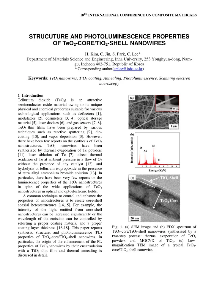
Fig. 1. (a) SEM image and (b) EDX spectrum of coating layer thickness [16-18]. This paper reports TeO 2 -core/TiO 2 -shell nanorwires synthesized by a synthesis, structure, and photoluminescence (PL) two-step process: thermal evaporation of TeO 2 properties of TeO 2 -core/TiO 2 -shell nanowires. In powders and MOCVD of TiO 2 . (c) Low- particular, the origin of the enhancement of the PL magnification TEM image of a typical TeO 2 - properties of TeO 2 nanowires by their encapsulation core/TiO 2 -shell nanowire. with a TiO 2 thin film and thermal annealing is discussed in detail.

  2. 3 Results and discussion 2 Experimental Fig. 1a shows the FE-SEM image of the TeO 2 - TeO 2 -core/TiO 2 -shell one-dimensional (1D) core/TiO 2 -shell 1D nanostructures synthesized by a nanostructures were prepared by using a two-step two-step process comprising thermal evaporation process: thermal evaporation of Te powders and and MOCVD in this study. The core-shell nanowires metal organic chemical vapor deposition (MOCVD) were 40 - 140 nm in diameter and up to a few tens of of TiO 2 . The 1D nanostructures will be simply called micrometers in length. No globular particle was nanowires hereafter because most of the individual observed at the tip of a typical nanowire (inset in Fig. 1D nanostructures have a wire-like morphology as 1a) and no catalyst metal was detected in the EDX can be seen in SEM images later. First, TeO 2 spectrum (Fig. 1b) taken at the tip of a typical core- nanowires were synthesized on a p-type Si (100) shell nanowire marked by „ + ‟ (Fig. 1a). These two substrate in a quartz tube furnace by thermal facts suggest that the TeO 2 nanowires were not evaporation of Te powders at 400 o C in the air grown by a vapor-liquid-solid (VLS) mechanism but without using any metal catalyst and supplying any by a vapor-solid (VS) mechanism. The low- other gas. The thermal evaporation process was magnification TEM image exhibits the TeO 2 core at conducted for 1 h and then the furnace was cooled the center with a thickness of 60-70 nm and two down to room temperature. Next, the prepared TeO 2 TiO 2 shell layers with a thickness of 8-10 nm at both nanowires were transferred to an MOCVD chamber. edges of the TeO 2 core clearly (Fig. 1c). The TiO 2 The TiO 2 was deposited on the nanowires using the shell layers were not very uniform in thickness following method: The chamber was evacuated to a despite having been formed by MOCVD. base pressure of 135 mTorr. Titanium isopropoxide (TTIP) was used as a precursor for TiO 2 . N 2 at a flow rate of 30 sccm was employed as the carrier gas for TTIP during the coating process. At the beginning of the process, O 2 was flushed into the chamber at a flow rate of 4 sccm for approximately 2 s to help dissociate the TTIP. The substrate temperature, canister temperature, and mixture temperature were maintained at 350, 60, and 70 o C, respectively, and the chamber pressure was kept at 800 mTorr throughout the process. Subsequently, the prepared TeO 2 -core/TiO 2 -shell nanowires were optionally annealed at 650 o C for 1 h in an Ar atmosphere. The products were characterized by using field emission scanning electron microscopy (FESEM, Hitachi S-4200) equipped with an energy-dispersive X-ray spectrometer (EDXS). The high resolution TEM (HRTEM) images and the selected area electron diffraction (SAED) patterns were also taken on the same systems. Photoluminescence (PL) measurements and X- ray diffraction (XRD) analyses were performed Fig. 2. (a) Local HRTEM image of a typical TeO 2 - at room temperature on the products by using a core/TiO 2 -shell nanowire at the core-shell interface 325 nm He-Cd laser (Kimon, IK, Japan) as the region. (b) corresponding SAED pattern. excitation source and an X-ray diffractometer (Philips X‟pert MRD) with Cu -K α characteristic Several nanocrystallites were observed in the radiation, respectively. core region on the left hand side whereas no regular

  3. PAPER TITLE atomic arrangement was observed in the shell region thicknesses. The uncoated TeO 2 nanowires (0 h) on the right hand side of the HRTEM image taken exhibit a weak broad violet emission band centered from the interface region of the core-shell nanowires at approximately 430 nm. In contrast, the TiO 2 - (Fig. 2a). All the reflection spots on several coated TeO 2 nanowires (0.5-2.5 h) have an emission concentric circles in the corresponding SAED band at approximately 470 nm in the bluish violet pattern (Fig. 2b) were identified to be (121), (141), region. In other words, TeO 2 nanowires were slightly and (042) reflections of simple tetragonal-structured red-shifted by TiO 2 coating. Also, it appears that the TeO 2 with lattice constants a = 0.481 nm and c = intensity of the bluish violet emission from the core- 0.7613 nm (JCPDS No. 78-1713), indicating that the shell nanowires depends on the TiO 2 deposition time TeO 2 core on the lower side of the TEM image is strongly. The bluish violet emission tends to polycrystalline. The reflections from TiO 2 shell are increase very rapidly as the deposition time too weak to be observed, indicating that the as- increases from 0 to 1.5 h and then to decrease very deposited TiO 2 shell layer on the upper side of the rapidly with further increases in the deposition time TEM image is amorphous. The crystal structures of from 1.5 to 2.5 h. Consequently, the highest the core-shell nanowires was confirmed by the XRD emission intensity was obtained for a deposition diffraction pattern in Fig. 3. All the refection peaks time of 1.5 h (corresponding to a TiO 2 coating layer in the pattern fit to the simple tetragonal TeO 2 and thickness of ~10 nm) and its intensity was about 6 no peaks from TiO 2 shells are identified in the as- times as high as that of the violet emission from the synthesized nanowires. These observations confirm coated TeO 2 nanowires. that the cores and shells of the as-synthesized nanostructures are crystalline and amorphous, respectively. Also, comparison of the XRD pattern of the annealed nanowires with the as-synthesized ones reveals that the transformation of the TeO 2 from the α -TeO 2 phase (simple tetragonal structure) to the β -TeO 2 phase (orthorhombic structure) and the partial crystallization of TiO 2 shells have occurred during the annealing process in the cores and shells, respectively. Fig. 4. Room temperature-PL spectra of the TeO 2 - core/TiO 2 -shell nanowires with differentTiO 2 deposition times, i.e., different TiO 2 layer thicknesses. Regarding the PL properties of TeO 2 1D nanostructures, the as-synthesized TeO 2 nanowires have a violet emission band centered at approximately 425 nm with a shoulder at approximately 540 nm from the TeO 2 crystal grown by the Czochralski method [19]. On the other hand, Fig. 3. XRD patterns of as-synthesized and annealed the room temperature PL spectrum of TiO 2 1D TeO 2 -core/TiO 2 -shell nanowires. nanostructures is known to be typically dominated by a blue emission band centered at approximately Fig. 4 displays the PL spectra for TeO 2 - 480 nm [20,21]. Therefore, the bluish violet core/TiO 2 -shell nanowires with different deposition emission appears to be from the TiO 2 shell layer times for TiO 2 , i.e., different TiO 2 shell layer 3

Download Presentation
Download Policy: The content available on the website is offered to you 'AS IS' for your personal information and use only. It cannot be commercialized, licensed, or distributed on other websites without prior consent from the author. To download a presentation, simply click this link. If you encounter any difficulties during the download process, it's possible that the publisher has removed the file from their server.

Recommend


More recommend