Spatially resolved Raman spectroscopy on single- and few-layer - - PowerPoint PPT Presentation

spatially resolved raman spectroscopy on single and few
SMART_READER_LITE
LIVE PREVIEW

Spatially resolved Raman spectroscopy on single- and few-layer - - PowerPoint PPT Presentation

Spatially resolved Raman spectroscopy on single- and few-layer graphene D. Graf, F. Molitor, and K. Ensslin Zrich Solid State Physics C. Stampfer, A. Jungen, and C. Hierold, Micro and Nanosystems, ETH Zrich L. Wirtz, Institute for


slide-1
SLIDE 1

Spatially resolved Raman spectroscopy on single- and few-layer graphene

  • D. Graf, F. Molitor, and K. Ensslin

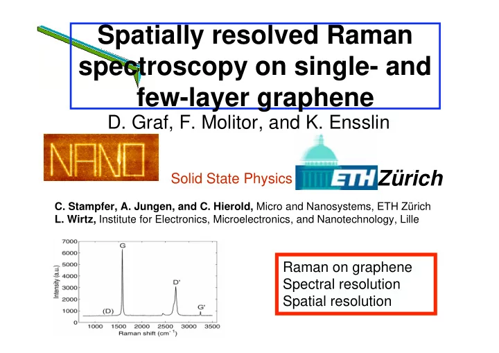
Raman on graphene Spectral resolution Spatial resolution Solid State Physics

Zürich

  • C. Stampfer, A. Jungen, and C. Hierold, Micro and Nanosystems, ETH Zürich
  • L. Wirtz, Institute for Electronics, Microelectronics, and Nanotechnology, Lille
slide-2
SLIDE 2

Ref.: Ludger Wirtz and Angel Rubio, Solid State Communications 131, 141 (2004)

Phonon spectrum of graphite

  • does the phonon spectrum depend on the number of layers ?
slide-3
SLIDE 3

Raman spectrum of graphite

  • does the phonon spectrum depend on the number of layers ?

EL=2.33eV

slide-4
SLIDE 4

Raman spectrum of graphite

k K

phonon at point, k~0 G, overtone G’ (1582 cm-1)

Single-resonant

EL=2.33 eV

k K

phonon close to K point, k>0 elastic scattering D (~1350 cm-1)

k K

2phonon close to K point, k>0 D‘ (~2700 cm-1)

Double-resonant

EL=2.33eV

slide-5
SLIDE 5

Spatial resolution: AFM

slide-6
SLIDE 6

Raman spectra of single- and double layer graphene

1 μm

1 1 2 SiO2 1 2

Scanning force microscope

1 μm

Scanning confocal Raman spectroscopy:

  • Laser excitation of 532 nm/

2.33 eV

  • Spot size:

D’ G

slide-7
SLIDE 7

Raman mapping: intensity of G-line

1 μm

1 1 2 SiO2 1 2

Scanning force microscope

1 μm

Scanning confocal Raman spectroscopy:

  • Laser excitation of 532 nm/

2.33 eV

  • Spot size:

two layers have higher G-line intensity, slightly different peak position

slide-8
SLIDE 8

Raman mapping: intensity of G-line

1 μm

1 1 2 SiO2 1 2

Scanning force microscope

1 μm

Scanning confocal Raman spectroscopy:

  • Laser excitation of 532 nm/

2.33 eV

  • Spot size:
slide-9
SLIDE 9

Raman mapping: position of G-line

slide-10
SLIDE 10

Raman spectra of single- and double layer graphene

1 μm

1 1 2 SiO2 1 2

Scanning force microscope

1 μm

Scanning confocal Raman spectroscopy:

  • Laser excitation of 532 nm/

2.33 eV

  • Spot size:

D’ G

slide-11
SLIDE 11

Raman mapping: FWHM of the D‘ line

1 μm

1 1 2 SiO2 1 2

Scanning force microscope

1 μm

Scanning confocal Raman spectroscopy:

  • Laser excitation of 532 nm/

2.33 eV

  • Spot size:

two layers have broader G-line, different peak position

slide-12
SLIDE 12

Raman mapping: FWHM of the D‘ line

1 μm

1 1 2 SiO2 1 2

Scanning force microscope

1 μm

Scanning confocal Raman spectroscopy:

  • Laser excitation of 532 nm/

2.33 eV

  • Spot size:

two layers have broader G-line, different peak position Raman: FWHM of D‘ line

1 μm

slide-13
SLIDE 13

D‘ line for single layer graphene

Related work: A.C. Ferrari et al., cond-mat/0606284

slide-14
SLIDE 14

D‘ line for double layer graphene

Related work: A.C. Ferrari et al., cond-mat/0606284

slide-15
SLIDE 15

Detecting single layer graphene

slide-16
SLIDE 16

What about the D-line?

1 μm

1 1 2 SiO2 1 2

Scanning force microscope

1 μm

Scanning confocal Raman spectroscopy:

  • Laser excitation of 532 nm/

2.33 eV

  • Spot size:

D’ G

slide-17
SLIDE 17

Raman mapping: intensity of the D line

k

K

phonon close to K, M point, k>0 Momentum restoring: elastic scattering D

Double-resonant

1) Crystallite grain size, symmetry breaking [Tuinstra and Koenig, 1970] 2) Defects, disorder in general [Y. Wang et al, 1990] Scanning force microscope

1 μm

1 1 2 SiO2

Raman: Integrated D line intensity

1 μm

Symmetry breaking and defects at edges and boundaries, not within the flake.

slide-18
SLIDE 18

Raman mapping: position of D-line

1 μm

1 1 2 SiO2 1 2

Scanning force microscope

1 μm

Scanning confocal Raman spectroscopy:

  • Laser excitation of 532 nm/

2.33 eV

  • Spot size:

G D

slide-19
SLIDE 19

Raman mapping: intensity of G-line

slide-20
SLIDE 20

Raman mapping: relative intensity of G/D‘-line

slide-21
SLIDE 21

Conclusions

Experiment: Davy Graf, Françoise Molitor, and Klaus Ensslin Solid State Physics, ETH Zürich, Switzerland Christoph Stampfer, Alain Jungen, and Christofer Hierold Micro and Nanosystems, ETH Zürich, Switzerland Theory: Ludger Wirtz Institute for Electronics, Microelectronics, and Nanotechnology (IEMN), 59652 Villeneuve d'Ascq, France Raman: FWHM D‘ Raman: Intensity D

  • Raman spectroscopy:

an alternative to scanning force microscopy

  • Monolayer sensitivity

(single to double layer)

  • Defects/symmetry breaking

at the edge (not within the flakes)

  • D. Graf et al., cond-mat/0607562, submitted

Related work: A.C. Ferrari et al., cond-mat/0606284,

  • A. Gupta et al., cond-mat/0606593