
SLIDE 1
Office of Research and Development National Exposure Research Laboratory Office of Research and Development National Exposure Research Laboratory
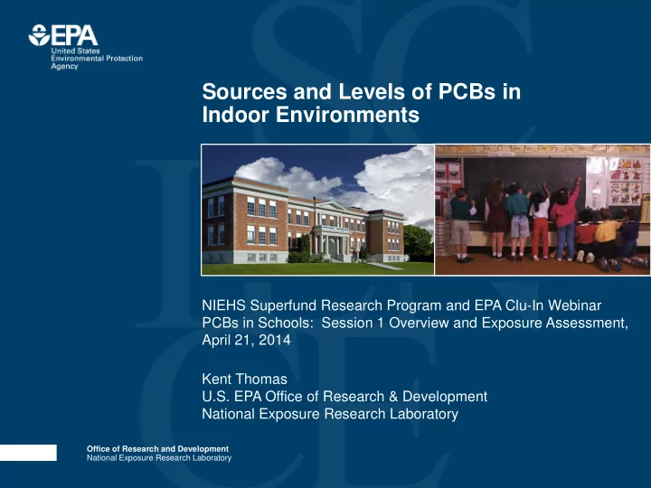
Sources and Levels of PCBs in Indoor Environments NIEHS Superfund - - PowerPoint PPT Presentation
Sources and Levels of PCBs in Indoor Environments NIEHS Superfund Research Program and EPA Clu-In Webinar PCBs in Schools: Session 1 Overview and Exposure Assessment, April 21, 2014 Kent Thomas U.S. EPA Office of Research & Development
Office of Research and Development National Exposure Research Laboratory Office of Research and Development National Exposure Research Laboratory
Office of Research and Development National Exposure Research Laboratory
2
Office of Research and Development National Exposure Research Laboratory
3
Office of Research and Development National Exposure Research Laboratory
4
Office of Research and Development National Exposure Research Laboratory
5
Office of Research and Development National Exposure Research Laboratory
6
Office of Research and Development National Exposure Research Laboratory
7
Office of Research and Development National Exposure Research Laboratory
8
Office of Research and Development National Exposure Research Laboratory
9
Office of Research and Development National Exposure Research Laboratory
10
Office of Research and Development National Exposure Research Laboratory
11
Office of Research and Development National Exposure Research Laboratory
12
Office of Research and Development National Exposure Research Laboratory
13
Office of Research and Development National Exposure Research Laboratory
14
Office of Research and Development National Exposure Research Laboratory
15
Office of Research and Development National Exposure Research Laboratory
16
Caulk Metal Door Frame Caulk - Door Frame Caulk - Bay Door Frame Estimated Total PCB Emission Rate (g/h)
200 400 600 800
School 2 Cafeteria Caulk - Door Frame Caulk - Bay Door Frame Estimated Total PCB Emission Rate (g/h)
200 400 600
School 2 Gymnasium C a u l k
F r a m e C a u l k
a l l P a n e l C a u l k
e t a l P a n e l Estimated Total PCB Emission Rate (g/h)
1000 2000 3000 4000
School 2 Corridor Caulk - Exterior Windows Estimated Total PCB Emission Rate (g/h)
200 400 600 800 1000
School 6 Classroom
Office of Research and Development National Exposure Research Laboratory
17
L
e s t E s t i m a t e d T
a l M e d i a n E s t i m a t e d T
a l H i g h e s t E s t i m a t e d T
a l Estimated Total PCB Emission Rate (g/h)
50 100 150 200 250 300
School 2 Classroom With 9 PCB Light Ballasts
Office of Research and Development National Exposure Research Laboratory
18
Locker Paint Wall Paint 1 Wall Paint 2 Ventilator Paint Pin Board Door Paint Ceiling Tile Floor Tile 1 Floor Tile 2 Chair PUF Foam Cove Molding Interior Window Glaze 1 Ventilator Gasket Foam Interior Window Glaze 2 Interior Joint Caulk Ventilator Insulation Door Window Glaze Wall Concrete Block
Estimated Total PCB Emission Rate (g/h)
10 20 30 40 50
School 6 Classroom 3
Office of Research and Development National Exposure Research Laboratory
19
Office of Research and Development National Exposure Research Laboratory
20
School Total PCBs in Air (ng/m3)
250 750 1500 2500 500 1000 2000
All 6 1 2 3 4 5 6
Air measurement distributions at 6 schools
90th 75th 50th 25th 10th
School Total PCBs in Surface Wipes (g/100cm2)
0.0 0.2 0.4 0.6 0.8 1.0 1.2 1.4 2.0 2.2 2.4 High-Contact Surfaces Low-Contact Surfaces
All 6 1 2 3 4 5 6
Surface wipe measurement distributions at 6 schools
Office of Research and Development National Exposure Research Laboratory
21
Air (ng/m^3)
500 1000 1500 2000 2500 3000
Wipe - High Contact (ug/100 cm^2)
0.0 0.5 1.0 1.5 2.0
Air ng/m^3
200 400 600 800 1000 1200
Dust (ppm)
20 40 60 80 100
Office of Research and Development National Exposure Research Laboratory
22
Office of Research and Development National Exposure Research Laboratory
23
1-CL 0.5% 2-Cl 13.4% 3-Cl 48.0% 4-Cl 32.7% 5-Cl 5.2%
Aroclor 1242
3-Cl 1.2% 4-Cl 16.3% 5-Cl 52.7% 6-Cl 26.8% 7-Cl 2.7%
Aroclor 1254
3-Cl 0.1% 4-Cl 10.5% 5-Cl 49.6% 6-Cl 34.8% 7-Cl 4.8% 8-Cl 0.2%
2-Cl 0.6% 3-Cl 4.3% 4-Cl 31.1% 5-Cl 51.1% 6-Cl 11.9% 7-Cl 0.8%
Indoor Air
Office of Research and Development National Exposure Research Laboratory
24
Aroclor 1254
PCB Congener Number
10 20 30 40 60 70 80 90 110 120 130 140 160 170 180 190 50 100 150 200
Aroclor 1254 Congeners (Weight Percents)
2 4 6 8 10
44 52 87 70 95 101 110 138 149 153 118 18 8 180 163 132 105 84 128
Aroclor 1254 Aroclor 1254
PCB Congener Number
10 20 30 40 60 70 80 90 110 120 130 140 160 170 180 190 50 100 150 200
Exterior Caulk Congener Concentration (ppm)
2000 4000 6000 8000 10000
44 52 87 70 95 101 110 138 149 153 118 18 8 180 163 132 105 84 128
Exterior Caulk Aroclor 1254
PCB Congener Number
10 20 30 40 60 70 80 90 110 120 130 140 160 170 180 190 50 100 150 200
Indoor Air Congener Concentration (ng/m3)
20 40 60 80 100
44 52 87 70 95 101 110 138 149 153 118 18 8 180 163 132 105 84 128
Indoor Air Aroclor 1254
PCB Congener Number
10 20 30 40 60 70 80 90 110 120 130 140 160 170 180 190 50 100 150 200
Indoor Dust Congener Concentration (ppm)
1 2 3 4
44 52 87 70 95 101 110 138 149 153 118 18 8 180 163 132 105 84 128
Indoor Dust
Office of Research and Development National Exposure Research Laboratory
25
Figure from 2009 NIEHS L. Birnbaum presentation
Office of Research and Development National Exposure Research Laboratory
26
0.01 0.1 1 10 100 1000 10000 20 40 60 80 100
Percentile Dose
0.01 0.1 1 10 100 20 40 60 80 100
Percentile Exposure
Exposure/Dose Profile
to t1 TI ME E X P.
D O S E
Ingestion
to t1 TI ME E X P.
D O S E
Dermal
to t1 TI ME E X P.
D O S E
Inhalation
Exposure Factor Distributions
20 40 60 80 100 1.0E-07 1.0E-06 1.0E-05 1.0E-04 1.0E-03 1.0E-02
Percentile Total Dose (mg/kg/day) Example Distributions of Estimated Doses
5th 50t h 95t h Annual average daily dose for Arsenic in warm climate from public playsets, home playsets, and decks
Office of Research and Development National Exposure Research Laboratory
27
Aroclor 1254 RfD = 0.020 µg/kg/day RfD Adjusted for Absorption = 0.017 µg/kg/day Median 64% Lower
6 – 10 year-olds
Office of Research and Development National Exposure Research Laboratory
28
Office of Research and Development National Exposure Research Laboratory
Ventilation Primary PCB Source Secondary PCB Sources and Sinks Dust/Soil
Office of Research and Development National Exposure Research Laboratory
30
Office of Research and Development National Exposure Research Laboratory
31
Office of Research and Development National Exposure Research Laboratory
32
Office of Research and Development National Exposure Research Laboratory
33
Office of Research and Development National Exposure Research Laboratory
34