Read Only Memory ROM A read only memory have address inputs and - - PowerPoint PPT Presentation

read only memory rom
SMART_READER_LITE
LIVE PREVIEW

Read Only Memory ROM A read only memory have address inputs and - - PowerPoint PPT Presentation

Read Only Memory ROM A read only memory have address inputs and data outputs With m address lines you can 2 m x n access the 2 m different ROM A m-1 memory addresses D n-1 A m-2 At each address, there is one D n-2 data word with n


slide-1
SLIDE 1

Read Only Memory ROM

William Sandqvist william@kth.se

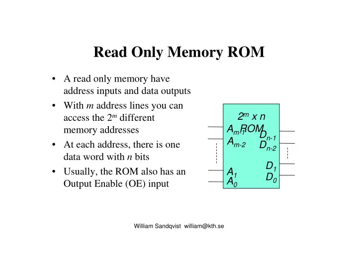
Am-1 Am-2 A0 A1 2m x n ROM Dn-1 Dn-2 D1 D0

  • A read only memory have

address inputs and data outputs

  • With m address lines you can

access the 2m different memory addresses

  • At each address, there is one

data word with n bits

  • Usually, the ROM also has an

Output Enable (OE) input

slide-2
SLIDE 2

Read Only Memory ROM

William Sandqvist william@kth.se

ROM 4M 512k × 8 bit Read only memory: Exemple of a ROM Chip Enable activates the chip Output Enable connects memory to outputs (otherwise they are in the three-state mode) OE CE

slide-3
SLIDE 3

A small ROM

William Sandqvist william@kth.se

A2 A0 A1 8x4 ROM D3 D2 D1 D0

A2 A1 A0 D3 D2 D1 D0 1 1 1 1 1 1 1 1 1 1 1 1 1 1 1 1 1 1 1 1 1 1 1 1 1 1 1 1

Possible memory content

slide-4
SLIDE 4

ROM

William Sandqvist william@kth.se

x0 x1 1 2 3 VDD GND GND GND Ord 0 Ord 1 Ord 2 Ord 3 OE z3 z2 z1 z0 Adress Innehåll x1x0 z3z2z1z0 00 1010 01 0101 10 1100 11 0001

OE=Output Enable Pullup ”1”

Address Content

slide-5
SLIDE 5

ROM implementation of combinatorical functions

William Sandqvist william@kth.se

Adress Innehåll xn-1…x1x0 zm-1…z1z0 0…00 1…10 0…01 0…01 … … 1…11 0…01

f(xn-1,…,x1,x0)

zm-1 … z1 z0 xn-1 … x1 x0

A ROM having n inputs with m outputs can be used to implement a combinatorial function with m outputs and 2n min-terms

Address Content

slide-6
SLIDE 6

ROM implementation of sequence circuit

William Sandqvist william@kth.se

With feedbacks a ROM can be used to generate sequences and implement state machines

Adress Innehåll xn-1…x3x2x1x0 zm-1…z3z2z1z0 0…0000 1…0001 0…0001 0…0010 … … 1…1111 0…0000

f(xn-1,…,x1,x0)

zm-1 … z4 z3 ... z0 xn-1 … x4 x3 ... x0

CP

A Moore-machine =

  • ne ROM and a

register with D-flip- flops

Address Content

slide-7
SLIDE 7

Read and Write Memory Random Access Memory RAM

William Sandqvist william@kth.se

  • RAM-memory has also

a Write (WR) input which allows us to enter a data word at a given address

  • Dn-1… D0 are both

inputs and outputs.

Am-1 Am-2 A0 A1 2m x n RAM Dn-1 Dn-2 D1 D0 WR OE

slide-8
SLIDE 8

Read-Write-Memory Random Access Memory RAM

William Sandqvist william@kth.se

Read/Write memory: SRAM 4M 512k × 8 bit WR RD CS Chip Select activates the chip RD read from memory, data outputs are active WR write to memory (at write the data outputs are in the three-state mode )

RD WR

slide-9
SLIDE 9

SRAM Static Random Access Memory

William Sandqvist william@kth.se

Sel Data

  • A SRAM-memory consits of a

matrix of SRAM-cells

  • To write ‘Data’ is used at

input!

– ‘Sel’ is set to 1 and the value that is on ‘Data’ is stored in the cell

  • To read ‘Data’ is used as
  • utput!

– ‘Sel’ is set to 1, and the value from the cell is present at the

  • utput

Strongest!

slide-10
SLIDE 10

SRAM

William Sandqvist william@kth.se

Sel 1 Sel 0 Data 0 Data 1

A matrix is formed by 2m x n SRAM-cells

slide-11
SLIDE 11

SRAM-memory

Sel 2 Sel 1 Sel 0 Sel 2

m 1

Read Write d d

n 1 –

d

n 2 –

q q

n 1 –

q

n 2 –

m

  • to-2

m decoder

Address a a

1

a

m 1 –

Data outputs Data inputs

tristate buffers are used to ensure that you just either reads or writes

William Sandqvist william@kth.se

slide-12
SLIDE 12

DRAM Dynamic RAM

William Sandqvist william@kth.se

  • SRAM memorycell needs 4 transistors and it

becomes too costly to implement a large memory

  • DRAM memorycell is using only one

transistor and one capacitor

slide-13
SLIDE 13

DRAM Memorycell

William Sandqvist william@kth.se

Word Line Bit Line 1-bit DRAM cell C

  • DRAM-cell consists of
  • nly one transistor and
  • ne capacitor
  • Skrivning

– To load the cell the word line is set to ‘1’

  • The cell now optains the

value from the bit line

slide-14
SLIDE 14

DRAM Memorycell

William Sandqvist william@kth.se

  • To read is a little bit more complex

– You do not want to lose the information when reading! – The bit-line is set at a voltage between the High and Low – To read the cell the word line is set to ‘1’

  • The bitline now adjusts it’s voltage to a

voltage up or down

  • An extra circuit (per bit line) senses the

current change direction to create a real 0 or 1

  • Aftervards the charge in the capacitor

C must be restored!

Word Line Bit Line 1-bit DRAM cell C

slide-15
SLIDE 15

DRAM Memory

William Sandqvist william@kth.se

Chip 256Mbit (32M×8) Memorymodule with 8 chips

slide-16
SLIDE 16

SRAM vs DRAM

William Sandqvist william@kth.se

  • SRAM takes up more space but a DRAM

requires a simpler access logic and is therefore faster (but also more expensive)

  • DRAM is used for random access memories in
  • ur regular computers
  • When you remove the power you loses the

contents of SRAM or DRAM memory!

slide-17
SLIDE 17

Memory types

William Sandqvist william@kth.se

  • Volatile memorys

– Memories lose their information if power is disconnected

  • static RAM (SRAM)
  • dynamic RAM (DRAM)
  • Non-volatile memorys

– Memories keep their information if power is disconnected

  • Flash (blockwise writing)
  • EPROM, EEPROM (bytewise writing)

We need a combination of different memories in an electrotechnical design!

slide-18
SLIDE 18

Flash-memory

William Sandqvist william@kth.se

  • Non-volatile memory
  • low cost and low power consumption
  • can be erased and updated but it takes much

more time than in a RAM-memory

slide-19
SLIDE 19

EPROM Erasable Programmable ROM

William Sandqvist william@kth.se

Programmable ROM (can be programmed with a chip programmer) Erasable - can be erased using ultraviolet light and then reprogrammed. Hence the "window" on the top side

  • f the chip.

When working with modern electronic equipment you will not have to meet the EPROM.

slide-20
SLIDE 20

William Sandqvist william@kth.se

Memory technologies

Technology

Accesstime

Cost $/GB SRAM 1 ns 1000 DRAM 50 ns 100 HDD 10 ms 1

Fast memory is expensive and inexpensive memories are slow!

Principle numbers.

slide-21
SLIDE 21

Logic in a microprocessor

William Sandqvist william@kth.se

There are both combinatorial and sequential logic in a

  • processor. Control logik is a statemachine while the

ALU are mostly combinatorial.

slide-22
SLIDE 22

Registry element

Din Dut WR Clock

>

WR

ut

D

in

D

WR = 1 synchronous writing WR = 0 hold Symbol hold WR /

William Sandqvist william@kth.se

1 logic element in a FPGA

slide-23
SLIDE 23

Register

> Symbol

WR

William Sandqvist william@kth.se

32 bit register is 32 logic elements in a FPGA

slide-24
SLIDE 24

Program counter -register

William Sandqvist william@kth.se

ADD MUX

> Clock

Register: hoppadress Program memory: Byteaddressed

”4”

Jump/Run

PC JA

Register: programräknare

An instruction is 4 bytes PC, Program Counter counts up with "4" after each instruction. At the program jumps PC is loaded with the jump address JA (Jump Address) and then the program continues from there.

32 bit instruktion

All processors have a program counter pointing out where the next instruction is to be fetched in the memory.

slide-25
SLIDE 25

Register with threestateoutpot

OE

> Symbol

WR

Symbol bidirectional (inputs and

  • utputs are connected together)

OE

>

WR

William Sandqvist william@kth.se

slide-26
SLIDE 26

Register and Databus

OE

>

WR OE

>

WR

Databus Several bidirectional registers with three state outputs can be connected to each other to form a common data bus. 1 1

William Sandqvist william@kth.se

slide-27
SLIDE 27

Register and Databuss

OE

>

WR OE

>

WR

Databus Data can now be controlled to be copied between all registers on the data bus. 1 1

William Sandqvist william@kth.se

slide-28
SLIDE 28

Dubble port register

OE1 OE2

> Symbol

WR

William Sandqvist william@kth.se

More Dubble portregisters can be paired with each

  • ther for two common output

buses.

slide-29
SLIDE 29

Mikrocomputer - architecture

William Sandqvist william@kth.se

The computer registers. A 32×32 bit dubbleport Register File

slide-30
SLIDE 30

Mikrocomputer - add

William Sandqvist william@kth.se

Example Add instruction

  • 1. The instruction

add R1,R2,R3 is fetched

from memory (as binary code)

  • 2. The instruction is decoded
slide-31
SLIDE 31

Mikrocomputer - add

William Sandqvist william@kth.se

Example Add instruction

  • 1. The instruction

add R1,R2,R3 is fetched

from memory (as binary code)

  • 2. The instruction is decoded
slide-32
SLIDE 32

Mikrocomputer - add

William Sandqvist william@kth.se

Example Add instruction

  • 3. Register R2 and R3 are add with

the ALU

  • 4. The Result is written to register

R1

slide-33
SLIDE 33

Mikrocomputer - add

William Sandqvist william@kth.se

it requires several clock pulse periods for the implementation of an instruction. (maybe you could arrange a Pipeline? ) Example Add instruction

  • 3. Register R2 and R3 are add with

the ALU

  • 4. The Result is written to register

R1

slide-34
SLIDE 34

Register file

The processor has a 32 × 32 bit register file (with dual port registers). It can therefore be simultaneously read from any two registers or write to a register per clock pulse. add R1, R2,R3

ADD R0 … R31 32×32 bit register file

The computer instruction add, means the sum R2+R3 is put in R1

William Sandqvist william@kth.se

A register file whith 32 registers are 322 = 1024 logic elements in a FPGA A 32 bit adder are 32 logic- elements in a FPGA

slide-35
SLIDE 35

Possible instruction format

William Sandqvist william@kth.se

add r1, r2, r3

5 bit 1 of 32 reg 5 bit 1 of 32 reg 5 bit 1 of 32 reg Operatingcode – we want to add

32 bit instruction

slide-36
SLIDE 36

William Sandqvist william@kth.se