Progress on a photosensor for the readout of the fast scintillation - - PowerPoint PPT Presentation

progress on a photosensor for the readout of the fast
SMART_READER_LITE
LIVE PREVIEW

Progress on a photosensor for the readout of the fast scintillation - - PowerPoint PPT Presentation

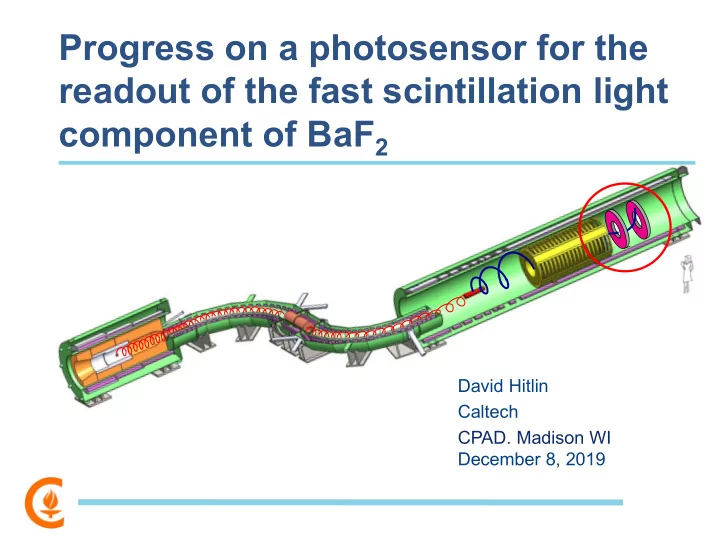
Progress on a photosensor for the readout of the fast scintillation light component of BaF 2 David Hitlin Caltech CPAD. Madison WI December 8, 2019 Photosensor options for BaF 2 readout BaF 2 has long been identified as an excellent choice


slide-1
SLIDE 1

David Hitlin Caltech

  • CPAD. Madison WI

December 8, 2019

Progress on a photosensor for the readout of the fast scintillation light component of BaF2

slide-2
SLIDE 2

Photosensor options for BaF2 readout

  • BaF2 has long been identified as an excellent

choice for a Mu2e (II) calorimeter, provided that

  • ne has a way of utilizing the 220 nm fast

component without undue interference from the 320 nm slow component

  • There are actually two fast components

(τ < 1 ns) at 195 and 220 nm and two slow components (τ = 630 ns) at 320 and 400 nm

  • Viable approaches:
  • Directly suppress the slow scintillation component
  • Interpose an external filter
  • Use a photosensor that is sensitive only to the fast component
  • Suppression of the BaF2 slow component by Y doping, as developed

by Zhu et al., is a major advance, although quite a bit of R&D remains

  • Is the resulting fast-to-slow component amplitude ratio already

sufficient to meet the rate and time resolution requirements of Mu2e-II?

  • If the consensus is “Yes”, I can perhaps conclude my presentation here
  • Dec. 8, 2019

David Hitlin CPAD Madison WI 2

slide-3
SLIDE 3

Photosensor options for Y-doped BaF2

  • I believe we still lack an ideal photosensor for the rates of Mu2e-II
  • What is required of an appropriate photosensor?
  • Spectral sensitivity in the 200 nm region for best energy and time

resolution

  • Fast/slow component discrimination for high rate capability
  • Improved rise/fall time characteristics to fully capitalize on

the fast component native time resolution and rate capability

  • Radiation hardness (photons/neutrons)
  • Photosensor candidates
  • Large area SiPMs developed for the MEG upgrade, DUNE, …

having ~25% PDE at 220nm (these already exist – e.g., Hamamatsu, FBK,,)

  • Large area delta-doped APDs with an integrated filter, having 50% PDE at

220nm and strong suppression at 320nm developed at Caltech/JPL/RMD

  • These have larger dark current and more noise than standard RMD

devices, but can be run at reduced temperatures

  • Large area SiPMs with an integrated filter and potentially improved time

response are currently under development at Caltech/JPL/FBK

  • Affordable MCPs, i.e., LAPPDs
  • Dec. 8, 2019

David Hitlin CPAD Madison WI 3

slide-4
SLIDE 4

Hamamatsu VUV MPPC

S1337 13370 0 ser eries

  • High P

gh PDE i in n VUV w wav avel elength h range ange

  • No slow/fas

ast compon

  • nent

ent discriminat nation

  • n
  • Low

Low opt

  • ptical

al c cros

  • sstalk

thr hrough gh t tren ench s structure

  • Typi

pical al dec decay ay time e of

  • f a

a lar arge ge ar area dev ea device, di dictated d by by RC RC

  • 4@

4@ 6x 6x6m 6mm

  • Work a

at c cryogen genic t temper perat atures es

Series/parallel connection of 6x6 mm SiPMs, as in the current Mu2e calorimeter, improves decay time characteristics

  • Dec. 8, 2019

David Hitlin CPAD Madison WI 4

slide-5
SLIDE 5

PMT + external filter

  • The TAPS experiment at ELSA at Mainz (no B field) has for many

years had a BaF2 forward calorimeter, reading out both fast and slow components with HR2059-01 PMTs

  • They use an integration time of 2µs; they are thus

limited to a single crystal rate of ~100kHz

  • An upgrade must cope with increased rates, so they

eliminate the slow component using a bandpass filter centered at 214 nm with a transmission at λmax that varies from 36 to 42%

  • Elimination of the slow component allows a gate of 20ns,

with a resulting single crystal rate capability up to ~2 MHz

  • An external filter can also be used with an appropriate solid state photosensor

However, an filter integrated with the silicon sensor can achieve greater efficiency

  • S. Diehl, R.W. Novotny,
  • B. Wohlfahrt and R. Beck,

CALOR 2014

  • Dec. 8, 2019

David Hitlin CPAD Madison WI 5

slide-6
SLIDE 6

137Cs line (662 keV) on BaF2 (1cm3)

PMT 9813 PMT 9813 25 ns gate Hamamatsu S13372 1000 ns gate PMT 9813 200W2D filter

  • Dec. 8, 2019

David Hitlin CPAD Madison WI 6

slide-7
SLIDE 7

Integrated approaches

  • The LAPPD, a channel plate PMT that works in a magnetic field, is very fast

and potentially very attractive, but a great deal of R&D remains before we have practical device for use with BaF2

  • Need either a photocathode with an extended UV response and a

quartz entrance window (i.e., no filter), or

  • An efficient filter and/or wavelength-shifting coating on the window
  • A size appropriate to the scintillating crystal Molière radius
  • An affordable price
  • DH and RYZ had initiated an effort with ANL to develop an 8x8 cm

LAAPD with a Cs2Te UV-extended solar-blind photocathode

  • After preliminary discussions, this effort has been suspended
  • Dec. 8, 2019

David Hitlin CPAD Madison WI 7

slide-8
SLIDE 8
  • AlGaN photocathodes have UV sensitivity and are solar-blind
  • Have been used in astrophysics for years, QEopaque ~30% at 220 nm
  • Wide-band semiconductors such as AlGaN are radiation-hard
  • Could be used as photocathodes

for MCP devices

  • An interference filter could be incorporated

U.Schühle, J.-F.Hochedez, "Solar-Blind UV detectors", ISSI Scientific Report SR-009, ISBN: 978-92-9221-938-3 O.Siegmund et al, Proc.SPIE 7021,70211B, 2008, doi:10.1117/12.790076

AlGaN photocathodes for an MCP

  • Dec. 8, 2019

David Hitlin CPAD Madison WI 8

slide-9
SLIDE 9

Integrated approaches

  • The LAPPD, a channel plate PMT that works in a magnetic field, is very fast

and potentially very attractive, but a great deal of R&D remains before we have practical device for use with BaF2

  • Need either a photocathode with an extended UV response and a

quartz entrance window (i.e., no filter), or

  • An efficient filter and/or wavelength-shifting coating on the window
  • A size appropriate to the scintillating crystal Molière radius
  • An affordable price
  • A large area APD, with delta-doping for improved speed and QE, and an

integrated ALD-applied interference filter

  • Devices have been produced, but noise is large at room temperature
  • A large area SiPM, with delta-doping (a super-lattice) for improved speed and

QE, and an integrated ALD-applied interference filter

  • Development is underway
  • We made an abortive attempt with Hamamatsu
  • We have an ongoing effort with JPL/FBK
  • Note that delta-doping and ALD filter application are independent processes
  • Dec. 8, 2019

David Hitlin CPAD Madison WI 9

slide-10
SLIDE 10

Superlattice structures

  • JPL has developed superlattice structures

that provide greatly enhanced quantum efficiency and improved time response for photosensors

  • Delta-doping and superlattices have

been successfully employed for many years to enhance the UV performance

  • f CCDs and APDs used in UV

astronomy in satellites and balloons

  • Monoatomic layers of boron are implanted

beneath the (thinned) photosensitive surface of the Si device using molecular beam epitaxy (MBE) (2D doping)

  • The MBE layers allow the conduction

band to remain stable with varying surface charge

  • Dec. 8, 2019

David Hitlin CPAD Madison WI 10

slide-11
SLIDE 11

Superlattice performance improvements

  • Recombination of photoelectrons is

suppressed by quantum exclusion, resulting in close to 100% internal QE

  • Quantum efficiency in the 200-300 nm

region approaches the silicon transmittance (1-R) limit

  • Elimination of the undepleted region before

the avalanche structure substantially improves APD time performance over normal 9mm RMD device

  • This should work with SiPM structure as well
  • Both rise time and decay time are improved
  • The superlattice structure provides

stability under intense UV illumination

  • Relevant regime is ~ 1-10 J/cm2

Superlattice: rise time 6ns Unmodified: rise time 20ns RMD 9x9mm APD

  • U. Arp et al., J. Elect. Spect. and Related

Phenomena, 144, 1039 (2005)

  • Dec. 8, 2019

David Hitlin CPAD Madison WI 11

slide-12
SLIDE 12

ALD antireflection filters improve QE

The ALD technique can also be used to make a bandpass filter

slide-13
SLIDE 13

Three and five layer filters have been investigated

The “wider” five layer filter encompasses more of the 195 nm peak and provides improved slow component suppression Filter characteristics vary with angle

  • f incidence
  • J. Hennessey JPL

ALD bandpass interference filters

  • Dec. 8, 2019

David Hitlin CPAD Madison WI 13

slide-14
SLIDE 14

Three and five layer filters have been investigated

The “wider” five layer filter encompasses more of the 195 nm peak and provides improved slow component suppression

5 10 15 20 25 30 35 40 200 300 400 500 Quantum Efficiency (%) Wavelength (nm)

Measured QE on APD at zero bias QE ~ doubles at nominal gain

  • J. Hennessey JPL

ALD bandpass interference filters

  • Dec. 8, 2019

David Hitlin CPAD Madison WI 14

slide-15
SLIDE 15

BaF2 fast/slow component comparison

fast:slow Produced 0.176 Detected 3.65 Improvement ~20

  • Dec. 8, 2019

David Hitlin CPAD Madison WI 15

slide-16
SLIDE 16

Fast/slow component comparison

fast:slow Produced 0.176 Detected 3.65 Improvement ~20

  • Dec. 8, 2019

David Hitlin CPAD Madison WI 16

slide-17
SLIDE 17

ALD filter with Y-doped BaF2 provides further suppression

  • Dec. 8, 2019

David Hitlin CPAD Madison WI 17

slide-18
SLIDE 18

SiPMs with ALD filter and/or delta doping

  • FBK SIPM

– Caltech and JPL are working with FBK to incorporate a 220nm filter on a large area SiPM and to also incorporate a superlattice – Many processed have been explored to remove or thin the usual SiNx passivation from individual cells – JPL has developed an appropriate interference filter that will be deposited at wafer level – FBK hasproduced 6x6mm chips for testing at Caltech

  • G. Paternoster FBK
  • J. Hennessey JPL
  • Dec. 8, 2019

David Hitlin CPAD Madison WI 18

slide-19
SLIDE 19

Filters built on measured passivation layer

  • Standard SiPM passivation is done with SiNx

– This limits filter design optimization due to strong UV absorption

  • We have therefore also made wafers with alternative passivation using SiO2

– allows a better match to the BaF2 fast component

  • Precise knowledge of the thickness of the passivation layer is required to

design an

  • ptimal filter

– Ellipsometry measurements at JPL confirm FBK thickness values – Nomimal filter design parameters are tweaked to actual passivation layer thickness

W1 test structures JPL meas. FBK meas. pt 1 29.25 28.78 pt 2 29.26 28.9 pt 3 29.36 29.09 pt 4 29.45 29.09 pt 5 28.58 28.29 pt 6 28.93 28.55 pt 7 29.3 28.92 pt 8 28.98 28.57 pt 9 29.48 29.16 std 0.3 0.3 avg 29.2 28.8

  • Dec. 8, 2019

David Hitlin CPAD Madison WI 19

slide-20
SLIDE 20

Wafer level production and processing

  • FBK has produced wafers with 6 mm x 6 mm SiPMs

(actually 4 internally interconnected 3 mm x 3mm structures (35µm pixels) with a several process variations

– Ion implantation after SiNx passivation – SiNx passivation as sacrificial layer before ion implantation, then removed and replaced – SiO2 passivation – Several SiNx and SiO2 thicknesses – Standard and with metal/poly guard ring structures

  • Six wafers have been processed at JPL

– SiNx passivation - apply filter – SiO2 passivation – apply filter – SiO2 passivation, no filter – delta-doped to improve QE and rise time

  • Dec. 8, 2019

David Hitlin CPAD Madison WI 20

slide-21
SLIDE 21

Structure # 35um_std 231 35um_RqM 231 Test Structure 22

  • rigin

Mask alignment markers

(Filter etching as post- processing step)

  • rigin

Test Structures

Wafer Layout

Wafer level production and processing

  • Dec. 8, 2019

David Hitlin CPAD Madison WI 21

slide-22
SLIDE 22

Filter options with updated optical models

  • Three layer and five layer structures in which the first layer is either SiO2 or SiNx
  • All layers are thin enough that there is little advantage in moving to the higher
  • rder filters

– The increased loss in the SiNx makes it difficult to have significant throughput below 200 nm

silicon

SiNx 25 nm Al – 13 nm Al2O3 – 28 nm Al – 10 nm Al2O3 – 12 nm

Examples:

3 layer on SiNx 5 layer on SiNx 3 layer on SiO2 5 layer on SiO2

2nd order version:

silicon

SiO2 37 nm Al – 18 nm Al2O3 – 30 nm Al – 11 nm Al2O3 – 20 nm Al2O3 – 60 nm

First order on SiNx Second order on SiO2

  • J. Hennessey JPL
  • Dec. 8, 2019

David Hitlin CPAD Madison WI 22

slide-23
SLIDE 23

Next steps

  • After the ALD filters (and, eventually, superlattice structures) are created

at JPL, the wafers are returned to FBK for probing and dicing into chips

  • Chips with differing filters and with and without superlattices are being

tested at Caltech for filter performance and QE and then spectra will be taken with pure and Y-doped barium fluoride crystals – Our existing spectrophotometer has been modified to extend response to 200 nm

  • Radiation hardness studies and MTF studies

will follow

  • Additional wafers are available for further

rounds with modified parameters

  • Measured QE of a five-layer filter on a

device that was not brought to full bias, resulting in surface recombination and incomplete charge collection

  • Dec. 8, 2019

David Hitlin CPAD Madison WI 23

slide-24
SLIDE 24

Conclusions

  • A very fast barium fluoride crystal calorimeter that exploits the fast scintillation

component for its high rate capability and excellent time resolution is an appropriate component of a Mu2e-II upgrade or other high rate experiments

  • Y-doped BaF2 provides very significant suppression of the 320 nm slow

component with little effect on the 220 nm fast component

  • In order to fully exploit the < 1ns decay time of the fast component for improved

rate capability and time resolution, better photosensors are required and several are under development

  • Desired device characteristics
  • High gain
  • High QE for the 220nm BaF2 fast component
  • Insensitive to the 320nm BaF2 slow component
  • Excellent rate performance
  • UV stable
  • Radiation hard to γs and neutrons
  • A SiPM with these performance characteristics is in development
  • Other promising technologies may yet emerge
  • Dec. 8, 2019

David Hitlin CPAD Madison WI 24