Processor Datapath Levels in Processor Design We can talk about - - PowerPoint PPT Presentation

processor datapath levels in processor design
SMART_READER_LITE
LIVE PREVIEW

Processor Datapath Levels in Processor Design We can talk about - - PowerPoint PPT Presentation

Processor Datapath Levels in Processor Design We can talk about design at a variety of levels (from low to high): Circuit design: transistors, resistors, capacitors, etc. Building gates, flip-flops, etc. Logic design: putting gates


slide-1
SLIDE 1

124 CSE378 WINTER, 2001

Processor Datapath

125 CSE378 WINTER, 2001

Levels in Processor Design

  • We can talk about design at a variety of levels (from low to high):
  • Circuit design: transistors, resistors, capacitors, etc. Building

gates, flip-flops, etc.

  • Logic design: putting gates (AND, OR, XOR, etc) and flip-flops

together to build blocks such as registers, adders, memory. See CSE370.

  • Register transfer level: describes the execution of instructions by

showing how information is transferred and manipulated between adders, registers, memory, etc.

  • Processor description: the ISA.
  • System description: includes memory hierarchy, IO, number of

processors, etc.

126 CSE378 WINTER, 2001

Register Transfer Perspective

  • We’ll use either block diagrams or pseudocode to describe the
  • peration/design of a simple processor which implements a

subset of the MIPS ISA.

  • We’ll implement just a subset of the ISA:
  • Memory reference: lw and sw
  • Arithmetic: add, sub, and, or, stli
  • Control: beq, jump
  • Key components:
  • Combinational: the output is a function of the inputs (e.g. an

adder)

  • Sequential: state is remembered (e.g. a register)

127 CSE378 WINTER, 2001

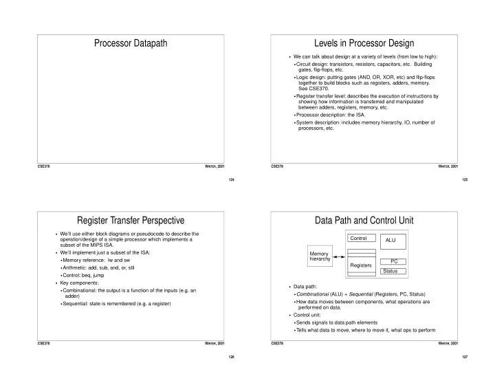
Data Path and Control Unit

  • Data path:
  • Combinational (ALU) + Sequential (Registers, PC, Status)
  • How data moves between components, what operations are

performed on data.

  • Control unit:
  • Sends signals to data path elements
  • Tells what data to move, where to move it, what ops to perform

PC Status ALU Control Registers Memory hierarchy

slide-2
SLIDE 2

128 CSE378 WINTER, 2001

Combinational Elements: ALU

  • ALU computes (combinational) output from its two inputs.
  • Performs functions needed to execute arithmetic and logical

instructions.

  • Combinational logic has a “critical path” which determines the

length of time needed for the output to stabilize given stable

  • inputs. (These days: ~1ns).

ALU ALU

  • peration

Input 1 Input 2 Output 129 CSE378 WINTER, 2001

Synchronous Design

  • Use a periodic clock, which controls when signals can be read

and when they can be written. Values in storage elements can

  • nly be updated on clock edges.
  • The clock determines when events occur, ie, when signals sent by

control unit are obeyed in the datapath.

State Element 1 State Element 2 Combinational Logic State Element 1 State Element 2 Combinational Logic write signal write signal

Changes occur on every clock edge: Changes occur on clock edges when a write signal is asserted (this allows combinational logic to take several cycles):

130 CSE378 WINTER, 2001

Building Blocks: Storage elements

  • The basic building block is the register.
  • Our registers store 32 bits.
  • A register will only be written on the clock edge AND when the

write control line is asserted.

  • It can be read and written on the same clock, but the value read

will be the OLD value.

Write control Output bus Input bus 131 CSE378 WINTER, 2001

Building Blocks: Register File

  • Register file is an array of registers (32 in MIPS)
  • ISA tells us that we should be able to read 2 registers and write 1

register in a given instruction.

  • We need to know which registers to read/write, and what data to

write.

  • Typical access time is around 1ns.

Registers Read reg 1 Read reg 2 Write reg Write data Read data 1 Read data 2 Write control

slide-3
SLIDE 3

132 CSE378 WINTER, 2001

Memory

  • Memory is like a register file, but much larger and slower.
  • Can only read or write one location per cycle.
  • Typical access time (for primary memory) is around 50ns. For

cache memory it is closer to 5ns.

Memory Read address Write address Write data Read data 1 Write control Read control 133 CSE378 WINTER, 2001

Instruction Fetch Datapath

  • Our implementation will fully execute one instruction per clock

cycle: single cycle implementation.

  • The PC tells us the read address.
  • On each clock edge, a new value for PC will be latched into the

PC register.

Instruction Read address PC Adder Memory 4 Instruction 134 CSE378 WINTER, 2001

Datapath for R-type Instruction

  • The instruction bits name the read and write regs (rs, rt, rd).
  • On the clock edge, the data is read, which moves through the

ALU, hopefully in time to be latched into the write port at the next clock edge.

Registers Read reg 1 Instruction reg 2 Write reg Write data Read data 1 Read data 2 Write control ALU ALU

  • peration

Read 135 CSE378 WINTER, 2001

Datapath for Load/Store

  • The instruction bits tell us the registers to use (src/dest and base

register) and the 16 bit signed offset.

  • We use the ALU to compute the effective address, which is

passed along to the data memory.

Registers Read reg 1 Instruction Write reg Write data Read data 1 Read data 2 Write control ALU ALU

  • peration

16 32 Sign Ext. Memory Read address Write address Write data Read data 1 Write control Read control Read reg 2

slide-4
SLIDE 4

136 CSE378 WINTER, 2001

Datapath For Branch

  • Question: Why can’t we just use the ALU to compute the branch

target address?

Registers Read reg 1 Instruction reg 2 Write reg Write data Read data 1 Read data 2 Write control ALU ALU

  • peration

Read 16 32 Sign Ext. Adder Sum PC + 4 Shift Left 2 Branch Target To branch control logic 137 CSE378 WINTER, 2001

Combinational Elements: (De)Multiplexor

  • Multiplexor (mux) selects the value of one of its inputs to be

routed to the output:

  • Demultiplexor routes its input to one of its outputs:

M U X Select control signal Output 2 or more inputs D M U Select control signal 2 or more input

  • utputs

X 138 CSE378 WINTER, 2001

Combining Memory and R-type

  • Note that we add 2 muxes:
  • One to select the second ALU input
  • One to select the source for the register writeback (memory or

ALU result)

Registers Read reg 1 Instruction reg 2 Write reg Write data Read data 1 Read data 2 Write control ALU ALU

  • peration

Read 16 32 Sign Ext. Read address Write address Write data Read data Write control Read control

m u x

Memory

m u x

139 CSE378 WINTER, 2001

Adding Instruction Fetch

Registers Read reg 1 reg 2 Write reg Write data Read data 1 Read data 2 Write control ALU ALU

  • peration

Read 16 32 Sign Ext. Read address Write address Write data Read data Write control Read control

m u x

Memory

m u x

Instruction Read address PC Adder Memory 4 Instruction

slide-5
SLIDE 5

140 CSE378 WINTER, 2001

Full Datapath: Adding Branches

Registers Read reg 1 reg 2 Write reg Write data Read data 1 Read data 2 Write control ALU ALU

  • peration

Read 16 32 Sign Ext. Read address Write address Write data Read data Write control Read control

m u x

Memory

m u x

Instruction Read address PC Adder Memory 4 Instruction Adder Shift Left 2

m u x

141 CSE378 WINTER, 2001

Processor Control

142 CSE378 WINTER, 2001

Adding Control

  • Control Unit:
  • Decodes instruciton opcode/function field
  • Sends signals to the data path (muxes, reg file, memories)
  • Some controls come directly from the instruction:
  • Register fields indicate which register to read/write
  • Immediate field
  • Building the control unit is not that complicated:
  • Input signals (opcode/function) are specified by the ISA
  • Output signals can be identified easily from the opcode
  • We can use PLAs (see CSE370) to build hardwired control units

143 CSE378 WINTER, 2001

Review of Instruction Format

  • The opcode lives in bits 31-26
  • The two registers to read are always the rs (25-21) and rt (20-16)

registers

  • For a load/store, we find the base register in the rs field (25-21)
  • The 16 bit offset (for branch or load/store) is in 15-0
  • The destination register can be in one of two places:
  • Loads: rt field (20-16)
  • R-type: rd field (15-11)
  • This implies we’ll need a mux to select between these two fields.
slide-6
SLIDE 6

144 CSE378 WINTER, 2001

Where are control signals needed?

  • Register File:
  • RegDst - selects between rt and rd field as destination register

(different for Load-store than R-type)

  • RegWrite - do we want to write a register? (R-type, Load-store)
  • ALU:
  • ALUSrc - selects between immediate or register value as source

for ALU (different for R-type and I-type)

  • Also need to select kind of ALU operation (bits 0-5 is function)
  • Memory:
  • MemWrite - are we writing memory? (store instructions)
  • MemRead - are we reading memory? (load instructions)
  • MemToReg - selects between memory value or ALU output as

writeback to the register file

  • Branch - are we branching?

145 CSE378 WINTER, 2001

How are signals asserted?

  • Control unit gets the opcode. Decoding yields:
  • Control for the 3 muxes (RegDst, ALUSrc, MemToReg)
  • Signals for read/write memory
  • Signal for register write
  • Signal for branch (ANDed with output of ALU)
  • Signal to ALU Control unit
  • We also have a small control unit for the ALU, which takes the

signal from the main control unit, together with the funct field (5-0) from the instruction.

  • We’ll focus on the main control unit. The ALU control is similar.

146 CSE378 WINTER, 2001

Examples

  • Using the provided figure (5.22), fill in this table which specifies

the control signals for the various instructions:

Instr.

  • pcode

bits: 543210 Reg Dst ALU Src Mem to Reg Reg Write Mem Read Mem Write Br R-format 000000 lw 100011 sw 101011 beq 000100

147 CSE378 WINTER, 2001

Control Functions

  • We can express the functions for the control lines logically:
  • RegDst = !op5 AND !op2
  • ALUSrc = op5
  • MemtoReg = op5
  • RegWrite = !op2 AND !op3
  • MemRead = op5 AND !op3
  • MemWrite = op5 AND op3
  • Branch = op2
  • For our subset instruction set, this minimized logic is fine, but for

the full instruction set (64 opcodes), we’d want something more general: We would specify the truth table, and implement it using a PLA.