
SLIDE 1
CIS 371 (Martin): Single-Cycle Datapath 1
CIS 371 Computer Organization and Design
Unit 4: Single-Cycle Datapath Based on slides by Prof. Amir Roth & Prof. Milo Martin
CIS 371 (Martin): Single-Cycle Datapath 2
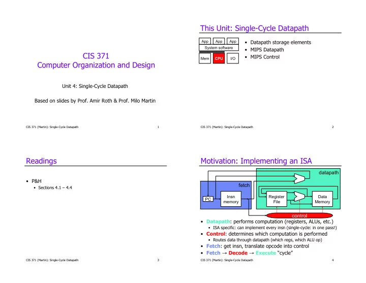
This Unit: Single-Cycle Datapath
- Datapath storage elements
- MIPS Datapath
- MIPS Control
CPU Mem I/O System software App App App
CIS 371 (Martin): Single-Cycle Datapath 3
Readings
- P&H
- Sections 4.1 – 4.4
CIS 371 (Martin): Single-Cycle Datapath 4
Motivation: Implementing an ISA
- Datapath: performs computation (registers, ALUs, etc.)
- ISA specific: can implement every insn (single-cycle: in one pass!)
- Control: determines which computation is performed
- Routes data through datapath (which regs, which ALU op)
- Fetch: get insn, translate opcode into control
- Fetch → Decode → Execute “cycle”