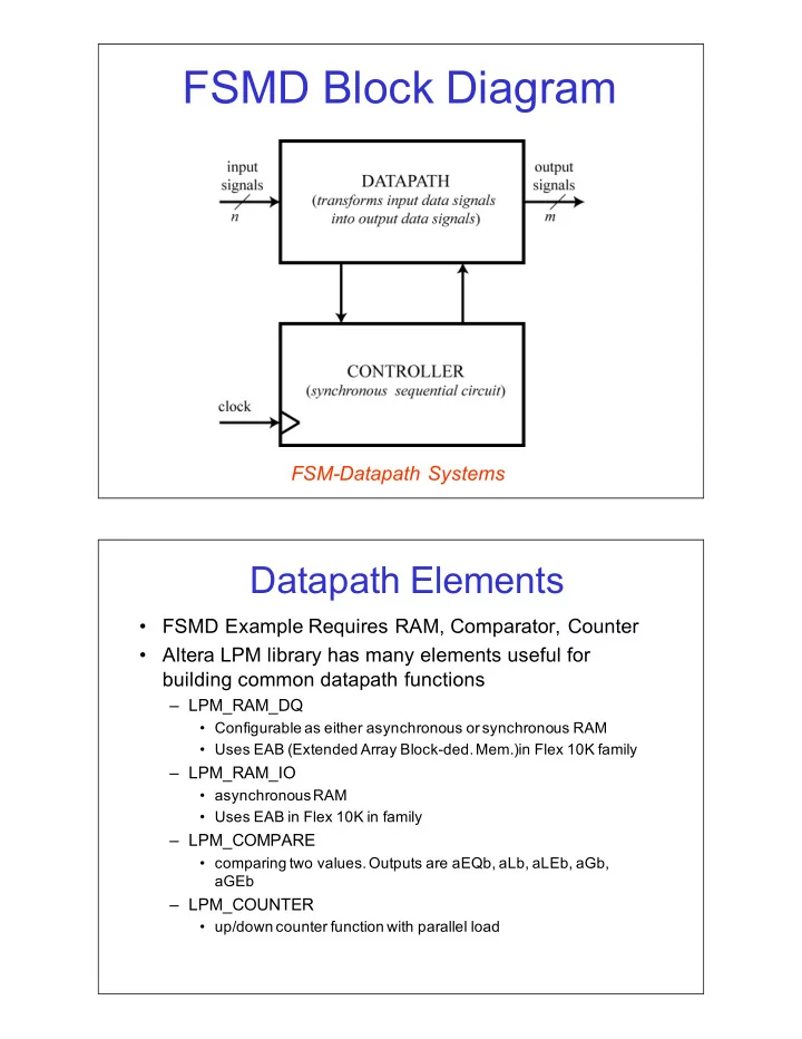
FSMD%Block%Diagram FSM$Datapath*Systems Datapath%Elements - - PDF document

fsmd block diagram
SMART_READER_LITE
LIVE PREVIEW

FSMD%Block%Diagram FSM$Datapath*Systems Datapath%Elements - - PDF document

FSMD%Block%Diagram FSM$Datapath*Systems Datapath%Elements FSMD%Example%Requires%RAM,%Comparator,%Counter Altera%LPM%library%has%many%elements%useful%for% building%common%datapath%functions LPM_RAM_DQ%%


slide-1
SLIDE 1

FSMD%Block%Diagram

FSM$Datapath*Systems

Datapath%Elements

  • FSMD%Example%Requires%RAM,%Comparator,%Counter
  • Altera%LPM%library%has%many%elements%useful%for%

building%common%datapath%functions

– LPM_RAM_DQ%%

  • Configurable%as%either%asynchronous%or%synchronous%RAM
  • Uses%EAB%(Extended%Array%BlockJded.%Mem.)in%Flex%10K%family

– LPM_RAM_IO%

  • asynchronous%RAM%%
  • Uses%EAB%in%Flex%10K%in%family

– LPM_COMPARE

  • comparing%two%values.%Outputs%are%aEQb,%aLb,%aLEb,%aGb,%

aGEb

– LPM_COUNTER

  • up/down%counter%function%with%parallel%load
slide-2
SLIDE 2

Controllers%in%FSMDs

  • The%job%of%the%finite%state%machine%is%to%sequence%
  • perations%on%a%datapath

R E G R E G

+

R E G

X

DIN DOUT FSM Control (reg load lines, mux selects)

Synchronous%vs%Asynchronous%RAM

  • Asynchronous%RAM

– combinational%element,%No%Clock%input – No%Clock – Data%available%after%propagation%delay%from%address – Address%MUST%BE%stable%while%WE%(write%enable)%is% high%so%that%only%ONE%location%is%written%too.%%Data%must% also%be%stable%during%write%cycle.

  • Synchronous%RAM

– sequential%element,%Clock%input%present – latches%input%data%and%control%lines%(address,%data)

slide-3
SLIDE 3

Counters%for%Driving%Address%Lines

WE%and%addr%can%Change%Close%in%Time

Delays%can%cause%WE%to%change%before%or%after%address.%%If% before,%then%can%write%to%both%LocA%and%LocB

slide-4
SLIDE 4

Sync%RAM%latches%address%and%WE

WE,%addr%latched%here Write%occurs%here

Use%Synchronous%RAM%when%Possible

  • Often%when%using%Asynchronous%RAM%generally%

end%up%latching%the%address,%WE,%and%din%anyway

  • Use%Synchronous%RAM%if%available%and%possible%

for%Application

  • In%Lab%exercises%and%Class%Examples,%will%always%

use/assume%synchronous%RAM

– Will%not%latch%output%data%unless%specifically%needed – Options%to%latch%control,%input%data,%output%data%available%

  • n%LPM_RAM_DQ
slide-5
SLIDE 5

Asynchronous%vs%Synchronous%Control

  • Many%LPMS%have%both%synchronous%and%

asynchronous%control%lines

– LPM_COUNTER%has%‘aload’%(asynchronous%load),%and% ‘sload’%(synchronous%load)\%%‘aclr’%and%‘sclr’%(async%and% sync%clear)

  • Always%use%a%Synchronous%control%line%if%possible,%

especially%if%connected%to%a%FSM%output.

– Any%glitch%on%an%asynchronous%control%line%can%trigger%it – If%using%a%FSM%output%for%an%asynchronous%control,%the%

  • utput%should%come%directly%from%a%FlipJFlop%output,%NOT%

from%combinational%gating.

Sample%FSMD%Design

  • Create%a%synchronous%RAM%block%that%

has%a%‘zeroing’%capability

  • If%external%‘zero’%input%asserted,%assert%

BUSY%output%and%zero%RAM%block

  • Load%a%LOW%and%HIGH%address%that%

specifies%the%memory%words%to%reset

  • Assume%RAM%size%is%64%x%8
slide-6
SLIDE 6

Memory%Zeroing%FSMD

RAM*&*External*Datapath Components

FSMD%Design%Steps

1) Define/Specify%Input/Output%Signals 2) Design%the%Datapath%Diagram 3) Define/Specify%Control%Signals 4) Design%the%Controller%ASM%Chart 5) Realize%Controller%in%HDL 6) Realize%Datapath%in%HDL%and/or%Schematic% Capture 7) Interconnect%Datapath%&%Controller 8) Validate%Design/Perform%Timing%Analysis

slide-7
SLIDE 7

FSMD%Input/Output%Signals

  • Inputs

! clk, reset ! low_ld J load%LOW%value%obtained%from%address%bus ! high_ld J load%HIGH%value%obtained%from%address%bus ! din[7..0] J data%bus%input%to%RAM ! addr[5..0] J address%bus%input%to%RAM%% ! zero J initiate%a%zero%cycle

  • Outputs

! dout[7..0] J memory%output%during%“normal”%operation ! busy J output%indicating%zeroing%operation%is%occurring

Datapath%Elements%%Needed

  • Two%registers%to%hold%LOW,%HIGH%value

– Use%LPM_DFF%or%write%Verilog%model%(reg6.v)

  • Need%a%6Jbit%counter%to%cycle%address%lines%of%

RAM

– LPM_COUNTER – Counter%needs%to%be%loaded%with%LOW%value%when%we% start%to%zero%the%RAM

  • Need%a%Comparator%to%compare%Counter%value%

and%HIGH%value%to%see%if%we%are%finished

  • Need%the%RAM%(use%LPM_RAM_DQ)
  • Multiplexers%(LPM_MUX%or%HDL)
slide-8
SLIDE 8

Datapath%Block%Diagram

Control*lines*are*not*shown*on*datapath*diagrams!!!

Required%FSM%Control%Signals

(examine%each%Datapath%component)

Registers:%Load%lines%for%LOW,%HIGH%registers%driven% externally%and%NOT%under%FSM%control. Counter:%%%sload%(synchronous%load),%cnt_en%(count% enable).%Counter%will%be%configured%to%only%count%up. Mux%Selects:%%When%doing%‘zero’%operation,%counter% will%be%driving%RAM%address%lines%and%RAM%input%data% line%will%be%zero.%The%same%select%line%can%drive%both% multiplexers. RAM:%%The%WE%of%the%RAM%needs%to%be%an%OR%of%the% external%WE%and%a%WE%that%is%provided%by%the%FSM.

slide-9
SLIDE 9

Control%Signals

Required%Controller%Operations

1) Wait%for%external%zero command% (controller%waits%for%‘zero’%input%to%be% asserted)%– RAM%in%“normal”%mode 2) Load%the%counter%with%the%LOW%address% value 3) Write%‘0’%data%value%to%RAM%via%address% specified%by%counter,%incrementing% counter%each%clock%cycle.%%Stop%writing% when%HIGH%register%value%equals% counter%value.

Three*DISTINCT*operationsA*need*3*control*STATES

slide-10
SLIDE 10

ASM%State%Definitions

  • Three%States
  • State%S0 waits%for%zero operation.%In%this%state%the%

external%addr and%din busses%are%multiplexed%to% RAM.%%Set%busy%flag%on%transition%to%State%S1.

  • State%S1 loads%counter%with%LOW%register%value
  • State%S2 does%zero%operation.%%Exit%this%state%with%

counter%value%equals%to%HIGH%register%value.%%On% state%exit,%clear%the%busy%flag%output%(conditional%

  • utput).%%

– Controller%requires%HIGHJLOW+1%clocks%in%this%state% (clear%LOW%to%HIGH%locations%inclusive)

Memory%Zeroing%ASM%Chart

slide-11
SLIDE 11

Memory%Zeroing%FSMD%Diagram

Design%Implementation

  • DESIGN%TASK:

– Specify/define%Input/Output%(often%this%is%in%prior% “spec”%phase) – Design%Datapath%(draw%datapath%diagram) – Specify%Controller%and%Datapath%Interface – Design%Controller%(draw%ASM%chart)

  • IMPLEMENTATION:

– Realize%Datapath%in%HDL%or%Schematic – Realize%Controller%(HDL%only%in%this%class) – Interface%Datapath%and%Controller%to%produce%FSMD Datapath$first*approach*is*my*preference*$ can*often*find*logic flaws*through*careful*consideration*of*datapath*before*worrying about*the*controller

slide-12
SLIDE 12

Design%Implementation%Guidelines

  • Perform%some%Intermediate%Validation%on%Datapath

– Datapath%Component%Hierarchy%can%be%Helpful

  • After%Datapath%is%finished,%Implement%Controller%in%HDL

– Initially%Specify%FSM%State%Value%as%External%Output%for%Debugging – Generate%Controller%HDL%directly%from%ASM%chart – Some%Intermediate%Validation%of%Controller

  • FSMD%Validate/Debug%J take%a%systematic%approach

– FSMD%will%USUALLY%NOT%WORK%the%first%time%J be%prepared%to% debug. – Attach%external%pins%to%as%many%internal%nets%as%possible%or%use%the% “logic%probe”%capability%to%observe%the%internal%net%values – Debug%FSMD%ONE%state%at%a%time%beginning%with%RESET%state.% – Do%not%test%the%next%state%until%the%current%state%works%as%expected.

Design%Implementation%Guidelines

  • Based%on%your%confidence%with%HDL,%decide%to%use%

LPM%components%versus%HDL%Specification%in% Datapath

  • Always%use%a%VERY%LONG%clock%cycle%to%start%out%

with%so%that%you%do%not%encounter%timing%problems

– Can%also%use%Functional%Simulation – To%be%absolutely%safe,%make%external%inputs%change%on% the%falling%edge%if%your%internal%logic%is%rising%edge% triggered%(this%gives%you%1/2%clock%of%setup%time).

slide-13
SLIDE 13

DATAPATH% COMPONENT% SPECIFICATION% USING%AN%HDL

Data%(D)%Latch

//HDL Example 5-1 //-------------------------------------- //Description of D latch (See Fig.5-6) module D_latch (Q,D,control);

  • utput Q;

input D,control; reg Q; always @ (control or D) if (control) Q = D; //Same as: if (control == 1’b1) Q = D; endmodule

D Q control No%default% assignment%for% ‘Q’\%only% assigned%when% gate%is%high.

slide-14
SLIDE 14

D FLIPJFLOP

//HDL Example 5-2 (adaptated-MAT) //----------------------- //D flip-flop module D_FF (Q,D,CLK);

  • utput Q;

input D,CLK; reg Q; always @ (posedge CLK) Q <= D; endmodule

DFF*with*Single* Synchronous*Input D Q

CLK

Rising%edge Assignment% ‘protected’%by% clock%edge.%So% DFF%is% synthesized.

Another*D FLIPJFLOP

//D flip-flop with asynchronous reset. //(adapted-MAT) module DFF (Q,D,CLK,RST);

  • utput Q;

input D,CLK,RST; reg Q; always @(posedge CLK or negedge RST) if (~RST) Q <= 1'b0; // Same as: if (RST == 1'b0) else Q <= D; endmodule

DFF*with*Single* Synchronous*Input and*Asynchronous reset*(RST) D Q

CLK RST

Assignment% after%rising%edge% clock%so%DFF%is% synthesized.

slide-15
SLIDE 15

JK and%T FLIPJFLOPS

//T flip-flop from D // flip-flop and gates module TFF (Q,T,CLK,RST);

  • utput Q;

input T,CLK,RST; wire DT; assign DT = Q ^ T ; //Instantiate the D flip- flop DFF TF1 (Q,DT,CLK,RST); endmodule //JK flip-flop from // D flip-flop and gates module JKFF (Q,J,K,CLK,RST);

  • utput Q;

input J,K,CLK,RST; wire JK; assign JK = (J & ~Q) | (~K & Q); //Instantiate D flipflop DFF JK1 (Q,JK,CLK,RST); endmodule

JK FLIPJFLOP

//HDL Example 5-4 (adapted-MAT) //---------------------------------- // Functional description

  • f JK flip-flop

module JK_FF (J,K,CLK,Q,Qnot);

  • utput Q,Qnot;

input J,K,CLK; reg Q; assign Qnot = ~ Q ; always @ (posedge CLK) case ({J,K}) 2'b00: Q <= Q; 2'b01: Q <= 1'b0; 2'b10: Q <= 1'b1; 2'b11: Q <= ~ Q; endcase endmodule

Description*Based*on*Characteristic*Table*Directly

slide-16
SLIDE 16

JK FLIPJFLOP

// Functional description of JK flip-flop // (adapted-MAT) module JK_FF (J,K,CLK,Q,Qnot,RST,PST);

  • utput Q,Qnot;

input J,K,CLK; reg Q; assign Qnot = ~ Q ; always @ (posedge CLK or negedge RST or negedge PST) if (~RST and ~PST) Q <= 1’bx; else if (~RST and PST) Q <= 1’b0; else if (~PST and RST) Q <= 1’b1; else case ({J,K}) 2'b00: Q <= Q; 2'b01: Q <= 1'b0; 2'b10: Q <= 1'b1; 2'b11: Q <= ~ Q; endcase endmodule

Comments%on%Examples

  • Modules%with%a%clock%in%sensitivity%list%are%called%%

‘clocked%modules’.

  • ALL%assignments%that%are%protected%by%a%clock edge%

will%have%a%DFFs%placed%on%the%logic%outputs.

  • posedge and%negedge Do%Not%Necessarily%Imply%

DFFs%will%be%Synthesized

  • Can%very%easily%insert%DFFs%between%blocks%of%logic%

(i.e.%pipelining)%in%Verilog

slide-17
SLIDE 17

Registers

The%most%common%sequential%building%block%is%the% register.%%A%register%is%N%bits%wide,%and%has%a%load%line%for% loading%in%a%new%value%into%the%register. DIN

N

CLK LD R E G DOUT

N

Register%contents%do%not% change%unless%LD%=%1%on% active%edge%of%clock. A%DFF%is%NOT%a%register!%DFF% contents%change%every%clock% edge.%% ACLR%used%to% asynchronously%clear%the% register ACLR

Verilog%for%8Jbit%Register

module reg8(dout,clk,reset,load,din); input [7:0] din; input clk, reset, load;

  • utput [7:0] dout;

reg [7:0] dout; always @(posedge clk or posedge reset) begin if (reset == 1’b1) dout <= 8’h00; else if (ld == 1’b1) dout <= din; end endmodule

Asynchronous% Reset Change%register% state%on%rising%edge% and%%assertion%of% load%line. No%default%clause% intentional%“inferred% storage”

slide-18
SLIDE 18

Pipelined%Datapath%Example

D Q C D Q C D Q C D Q C A B C D D Q C D Q C D Q C A_1 B_1 C_1 D_1 ABC_1 D_2 Y

Verilog%Module

module plogic (y, a, b, c, d, clk); input a, b, c, d, clk;

  • utput y;

reg y, a_1, b_1, c_1; reg d_1, d_2, abc_1; always @(posedge clk) begin a_1 <= a; b_1 <= b; c_1 <= c; d_1 <= d; end always @(posedge clk) begin abc_1 <= a_1 & b_1 & c_1; d_2 <= d_1; end always @(posedge clk); y <= abc_1 | d_2; endmodule

Each%always%block% defines%a%block%%of% logic%plus%DFFs. Logic%in%always% block%can%be%as% complex%as%you% wish.

slide-19
SLIDE 19

Always%Blocks

D Q C D Q C D Q C D Q C A B C D D Q C D Q C D Q C A_1 B_1 C_1 D_1 ABC_1 D_2 Y Block%1 Block%2 Block%3