Prevention of Sn whisker formation by surface treatment of Sn - - PDF document

prevention of sn whisker formation by surface treatment
SMART_READER_LITE
LIVE PREVIEW

Prevention of Sn whisker formation by surface treatment of Sn - - PDF document

GD - Goal is to find a thin coating that could be applied to pure Sn plating that would 1) prevent whiskers and 2) not significantly degrade solderability. Prevention of Sn whisker formation by surface treatment of Sn plating Part II Keun-Soo


slide-1
SLIDE 1

Prevention of Sn whisker formation by surface treatment of Sn plating Part II

Keun-Soo Kim,

Sun-Sik Kim, Seong-Jun Kim, Katsuaki Suganuma

ISIR, Osaka University

Masanobu Tsujimoto, and Isamu Yanada

  • C. Uyemura & Co., Ltd.

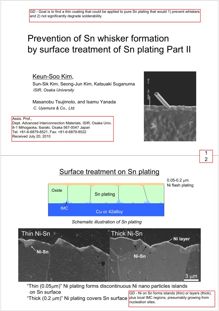
Surface treatment on Sn plating

Sn plating Cu or 42alloy

IMC Oxide 0.05-0.2 m Ni flash plating

Schematic illustration of Sn plating

Thin Ni-Sn Thick Ni-Sn

Ni-Sn Ni layer Ni-Sn

“Thin (0.05m)” Ni plating forms discontinuous Ni nano particles islands

  • n Sn surface

“Thick (0.2 m)” Ni plating covers Sn surface

GD - Goal is to find a thin coating that could be applied to pure Sn plating that would 1) prevent whiskers and 2) not significantly degrade solderability. GD - Ni on Sn forms islands (thin) or layers (thick), plus local IMC regions, presumably growing from nucleation sites.

  • Assis. Prof.,
  • Dept. Advanced Interconnection Materials, ISIR, Osaka Univ.

8-1 Mihogaoka, Ibaraki, Osaka 567-0047 Japan Tel: +81-6-6879-8521, Fax: +81-6-6879-8522 Received July 20, 2010

1 2

slide-2
SLIDE 2

Changes in whisker maximum length No whisker is formed on thick Ni/Sn plating Wetting behavior of various surface treatment samples

Wetting of thin Ni plating is equivalent to Sn plating while that of thick Ni is worse.

GD - Thin Ni seems to promote whisker growth (local compressive stresses?), but thick Ni completely suppresses whisker growth for at least 10,000 hrs (see slide 7 showing > 20,000 hrs) while uncoated and presumably similar specimens develop whiskers in < 1000 hrs. GD - Wetting balance zero-cross times shown as zero are actually infinite. Thick Ni destroyed solderability and was not further investigated.

3 4

slide-3
SLIDE 3

Experimental details

  • Materials1) pure Sn plating

( t:6m, current density: 5A/dm2 - 5.5min )

2) thin (0.05m) Au or Pd/Sn plating 3) thick (0.2m) Au or Pd/Sn plating

  • Electrode : Cu, 42alloy
  • Exposure at room temperature over 8000 hrs
  • Microstructure observation: TEM, SEM, XRD
  • Static indentation loading test (load:300g, )
  • Wetting test

As-plated Microstructure

GD - Specimens with pure Sn plating were the controls. Purpose was to see if a thin or thick coating of Au or Pd/Sn, presumably electrodeposited, would inhibit whisker growth yet preserve solderability.

5 6

slide-4
SLIDE 4

Thin Au Thin Au Thick Au Thick Au

Surface microstructure (Au-Sn/Cu)

Thick Ni Thick Ni Thin Ni Thin Ni

Cross sectional microstructure

Pure Sn plating Pure Sn plating Thin Ni Thin Ni-

  • Sn

Sn plating plating

Ni-Sn

Thin Au Thin Au-

  • Sn

Sn

7 8

slide-5
SLIDE 5

Au Sn

Thick Au-Sn/Cu

Sn

Au layer

200 200

  • Au

AuSn2 Sn AuSn AuSn2

2, Z=[110]

, Z=[110] _ _

110 001 111

Sn Pd

Sn

Pd layer

100 100

  • Pd

PdSn4 Sn

Thick Pd-Sn/Cu

GD - By the time of microstructure analysis, a substantial fraction of the thick Au has already reacted with the Sn to form IMC. GD - By the time of microstructure analysis, only a small fraction of the thick Pd has reacted with the Sn to form IMC.

9 10

slide-6
SLIDE 6

Room temperature exposure test

Surface microstructures after RT exposure for 8400 hrs

Thin Au Thin Au Thin Pd Thin Pd Thick Au Thick Au Thick Pd Thick Pd

11 12

slide-7
SLIDE 7

24 hrs 24 hrs 240 hrs 240 hrs

1mm

XRD analysis before/after RT exposure (thick Au)

Initial 576 hrs 2160 hrs

Au layer gradually changed to AuSn2 phase during R.T. exposure

result in the surface morphology was changed after long-term exposure.

Changes in whisker maximum length as function of time

No whisker is formed on thin and thick Au or Pd/Sn plating

GD - Au and Pd/Sn (thin or thick) suppressed whisker growth for as long as data were reported (~8000 hrs). GD - 200 nm Ni suppressed whisker growth for as long as data were reported (~3 yrs).

13 14

slide-8
SLIDE 8

Summarizing the Sn whisker formation behavior during R.T. exposure Pd Pd-

  • Sn

Sn Sn Sn

Pd-Sn/Cu or 42 alloy after RT exposure for 2160 hrs

Metal layers are very uniform and stable during R.T exposure, thus, it acts as protective layer of Sn whisker nucleation

  • n Sn plating surface.

As As-

  • plated

plated After 670 hrs After 670 hrs Growth of Growth of IMCs IMCs between between Sn Sn and Cu and Cu during RT exposure during RT exposure

Static indentation loading test

GD - Even though Pd-Sn IMC has formed after 3 mo. at RT a continuous layer of Pd remains.

15 16

slide-9
SLIDE 9
  • Plating: pure Sn(t:6m), thin and thick Ni, Au, Pd-Sn plating
  • Electrode: Cu, 42 alloy
  • Loading time: 24~240 hours

Experimental details

Weight: 300g

ZrO2 ball (0.9mm) Plating Electrode

Surface Observation (168 hrs)

Thin Thin Au/Cu Au/Cu Thick Thick Au/ Au/Cu Cu Thin Pd Thin Pd/Cu /Cu Thick Pd Thick Pd/ /Cu Cu 17 18

slide-10
SLIDE 10

Cu

Thin Pd Thin Pd/Cu /Cu

Cross sectional microstructure (168 hrs)

As plated As plated

Sn whiskers are formed at surface where the Pd layer is broken. X X X 42alloy X X X Cu 0.05 Pd/Sn X X X 42alloy 0.05 Au/Sn X X X Cu 20 m 10 m X 42alloy X X X Cu 0.05 Ni/Sn 20 m 20 m 20 m 42alloy 20 m 10 m 10 m Cu Sn 120hrs 72hrs 24hrs Electrode Plating

Changes in Sn whisker length (Thin layer)

Metal-Sn plating is much stable against Sn whisker formation

under external applied stress condition. 19 20

slide-11
SLIDE 11

Wetting test

Au Pd

Initial 105/100%RH-8hrs

Ni/Cu 0.2 Au/Sn A21 Cu 0.2 Au/Sn A11 Ni/Cu 0.05 Au/Sn A2 Cu 0.05 Au/Sn A1 Ni/Cu 0.2 Pd/Sn P21 Cu 0.2 Pd/Sn P11 Ni/Cu 0.05 Pd/Sn P2 Cu 0.05 Pd/Sn P1

Wetting behavior of various surface treatment samples

Initial 105/100%RH-8hrs Wetting balance method Solder: Sn-3Ag-0.5Cu Flux: RMA, Temp.: 245 ºC

21 22

slide-12
SLIDE 12

Summary

Au or Pd layer on Sn plating surface stop whisker formation during room temperature exposure. Thin and Thick Au or Pd plating form the continuous and uniform layer. Both Au and Pd platings form IMCs with Sn plating. Both Au and Pd platings has a great effect in suppressing Sn whisker formation under external indentation pressure. Wettings of Au or Pd plating are equivalent to Sn.

23