
SLIDE 1
PREPARATION STUDIES FOR THE SECONDARY ELECTRON EMISSION EXPERIMENTS - - PowerPoint PPT Presentation
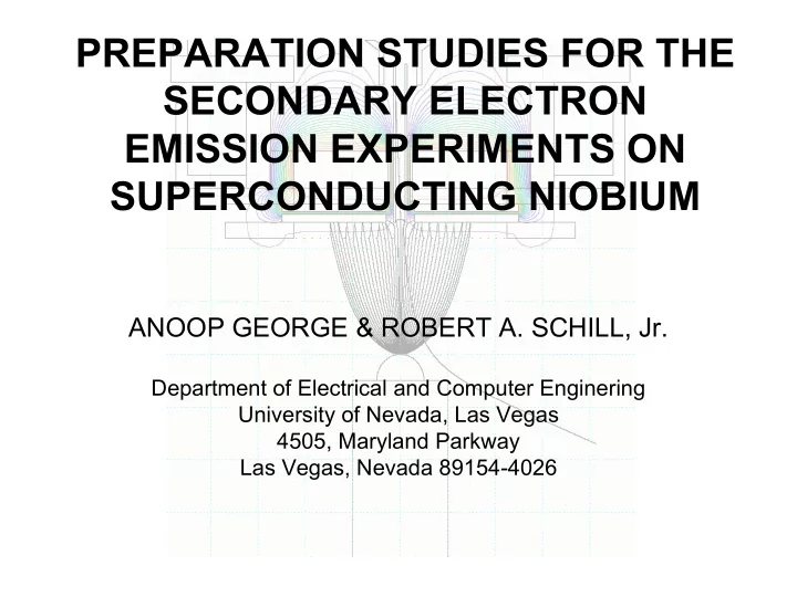
PREPARATION STUDIES FOR THE SECONDARY ELECTRON EMISSION EXPERIMENTS ON SUPERCONDUCTING NIOBIUM ANOOP GEORGE & ROBERT A. SCHILL, Jr. Department of Electrical and Computer Enginering University of Nevada, Las Vegas 4505, Maryland Parkway
Anoop George & Robert A. Schill, Jr. ANS Student Conference Madison, Wisconsin April 1-4, 2004. .
2
Anoop George & Robert A. Schill, Jr. ANS Student Conference Madison, Wisconsin April 1-4, 2004. .
3
Anoop George & Robert A. Schill, Jr. ANS Student Conference Madison, Wisconsin April 1-4, 2004. .
4
Anoop George & Robert A. Schill, Jr. ANS Student Conference Madison, Wisconsin April 1-4, 2004. .
5
0.20" 1.05" 0.75" 0.50" 0.92" Beam Line and Vertical Axis of Chambe Cryostat Axis M A V
Electron Gun
Detector
2.75 4.50" Cryostat
Anoop George & Robert A. Schill, Jr. ANS Student Conference Madison, Wisconsin April 1-4, 2004. .
6
Anoop George & Robert A. Schill, Jr. ANS Student Conference Madison, Wisconsin April 1-4, 2004. .
7
Anoop George & Robert A. Schill, Jr. ANS Student Conference Madison, Wisconsin April 1-4, 2004. .
8
2 2 2 2
2
2
s
X Y Z
Detector Secondary Electron Trajectories Niobium Target
φ θ
r
Anoop George & Robert A. Schill, Jr. ANS Student Conference Madison, Wisconsin April 1-4, 2004. .
9
ro
2 1 2 1 2 2
ro
2 1 2
2 1 / R
Anoop George & Robert A. Schill, Jr. ANS Student Conference Madison, Wisconsin April 1-4, 2004. .
10
1 2
1 2 1
flat
2
/ ~ R D D ∆ = ∆
0.050 49.77 0.24873 0.02 0.011 11.22 0.25082 0.001 0.091 0.046 45.55 0.22757 0.02 0.010 10.25 0.22920 0.001 0.111 .041 40.7 0.20369 0.02 0.0091 9.15 0.20481 0.001 0.143 0.038 38.36 0.19180 0.02 0.0085 8.56 0.19204 0.001 0.166 .035 35.3 0.17673 0.02 0.0079 7.94 0.17748 0.001 0.2 .029 28.9 0.14457 0.02 .00065 6.48 0.14497 0.001 0.333 θ [mrad.]
1
flat
Anoop George & Robert A. Schill, Jr. ANS Student Conference Madison, Wisconsin April 1-4, 2004. .
11
Anoop George & Robert A. Schill, Jr. ANS Student Conference Madison, Wisconsin April 1-4, 2004. .
12
Anoop George & Robert A. Schill, Jr. ANS Student Conference Madison, Wisconsin April 1-4, 2004. .
13
Anoop George & Robert A. Schill, Jr. ANS Student Conference Madison, Wisconsin April 1-4, 2004. .
14
Anoop George & Robert A. Schill, Jr. ANS Student Conference Madison, Wisconsin April 1-4, 2004. .
15
Anoop George & Robert A. Schill, Jr. ANS Student Conference Madison, Wisconsin April 1-4, 2004. .
16
Anoop George & Robert A. Schill, Jr. ANS Student Conference Madison, Wisconsin April 1-4, 2004. .
17