
SLIDE 1
8/26/2014 1
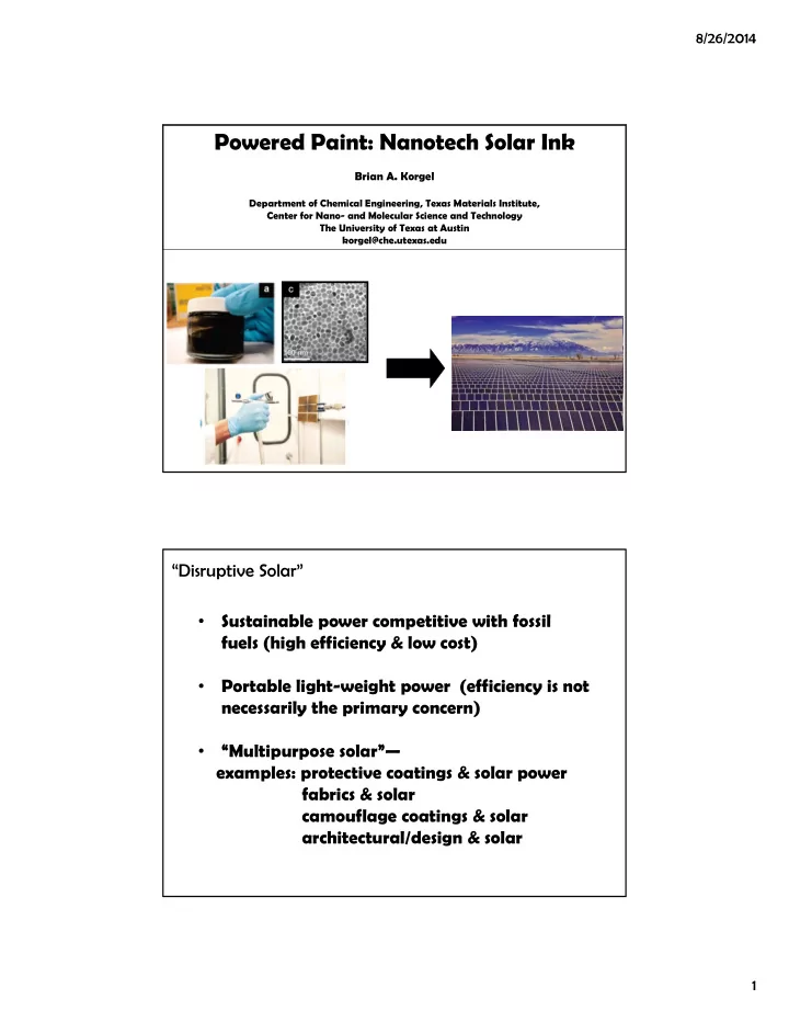
Powered Paint: Nanotech Solar Ink
Brian A. Korgel
Department of Chemical Engineering, Texas Materials Institute, Center for Nano- and Molecular Science and Technology The University of Texas at Austin korgel@che.utexas.edu
“Disruptive Solar”
- Sustainable power competitive with fossil
fuels (high efficiency & low cost)
- Portable light-weight power (efficiency is not
necessarily the primary concern)
- “Multipurpose solar”—