
SLIDE 1
18TH INTERNATIONAL CONFERENCE ON COMPOSITE MATERIALS
- 1. Introduction
After developed by O’Reagan and Grätzel in 1991 [1], dye sensitized solar cell (DSSC) is one of highly attractive solar cells for many applications such as flexible solar cell, and building integrated photovoltaics (BIPV) . Comparing DSSC with other solar cells, it has advantages such as low manufacturing cost, light weight, flexibility, transparency, and so on. DSSC consists of n-type semiconductor
- xide,
dye, electrolyte, and transparent electrodes. Conventional DSSC process is based on the glass substrate and it includes high temperature sintering process. This sintering process makes a strong bonding of oxide particles each other, but it limits the substrates materials of DSSC. Polymer substrates cannot be applied for the conventional DSSC fabrication process because of the process temperature. [2,3] Nano particle deposition system (NPDS) is a novel method to deposit ceramic and metallic powders on substrates at room temperature by accelerating particles to subsonic speeds [4]. This new method adopts advantages of cold-gas dynamic spraying (CGDS) and aerosol deposition (AD). In NPDS, compressed air transports particles from a powder feeder to nozzle and particles are accelerated by
- nozzle. The main advantage of DSSC fabrication by
using NPDS is that DSSC can be made on the polymer substrate and it needs no additional chemical processes. In addition, NPDS can create large oxide layer at once in atmospheric conditions. Previous research shows the successful fabrication results on DSSC using NPDS [5]. But it shows the possibility of fabrication and the energy conversion efficiency should be improved. In order to increase efficiency, the bonding between transparent electrode and semiconductor oxide layer and the structure of semiconductor oxide layer are important. The multi-layer structure of semiconductor oxide showed improved energy conversion efficiency in conventional DSSC fabrication process. Arakawa et al fabricated multilayer film structure DSSC to increase the efficiency [6]. But the preparation of TiO2 particles is complicated. In this paper, DSSC with polymer substrate was fabricated using NPDS by taking advantage of the room temperature process and no additional chemical process. The semiconductor oxide multi- layer was fabricated using two different sizes of TiO2 powders to increase the efficiency.
- 2. Experiment
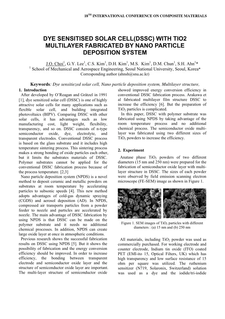
Anatase phase TiO2 powders of two different diameters (15 nm and 250 nm) were prepared for the fabrication of semiconductor oxide layer with multi- layer structure in DSSC. The sizes of each powder were observed by field emission scanning electron microscope (FE-SEM) image as shown in Figure 1.
500 nm
1 μm
(a) (b)
Figure 1. SEM images of TiO2 particles with different diameters : (a) 15 nm and (b) 250 nm
All materials, including TiO2 powder was used as commercially purchased. For working electrode and counter electrode, Indium tin oxide (ITO) coated PET (EMI-ito 15, Optical Filters, UK) which has high transparency and low surface resistance of 15
- hm per square was utilized. The ruthenium
sensitizer (N719, Solaronix, Switzerland) solution was used as a dye and the iodide/tri-iodide
DYE SENSITISED SOLAR CELL(DSSC) WITH TIO2 MULTILAYER FABRICATED BY NANO PARTICLE DEPOSITION SYSTEM
J.O. Choi1, G.Y. Lee1, C.S. Kim1, D.H. Kim1, M.S. Kim1, D.M. Chun1, S.H. Ahn1*
1 School of Mechanical and Aerospace Engineering, Seoul National University, Seoul, Korea*