
SLIDE 1
1
- Prof. S. Ben-Yaakov , DC-DC Converters
[10- 1]
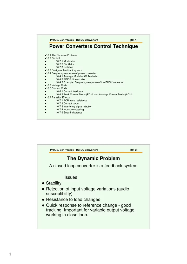
10.1 The Dynamic Problem 10.2 Control
- 10.2.1 Modulator
- 10.2.2 Oscillator
- 10.2.3 Isolation
10.3 Design of feedback system 10.4 Frequency response of power converter
- 10.4.1 Average Model – AC Analysis
- 10.4.2 SPICE Linearization
- 10.4.3 Example: Frequency response of the BUCK converter
10.5 Voltage Mode 10.6 Current Mode
- 10.6.1 Current feedback
- 10.6.2 Peak Current Mode (PCM) and Average Current Mode (ACM)
10.7 Parasitic Effects
- 10.7.1 PCB trace resistance
- 10.7.2 Correct layout
- 10.7.3 Interfering signal injection
- 10.7.4 Inductive coupling
- 10.7.5 Stray inductance
Power Converters Control Technique
- Prof. S. Ben-Yaakov , DC-DC Converters
[10- 2]
The Dynamic Problem
A closed loop converter is a feedback system Issues:
Stability Rejection of input voltage variations (audio
susceptibility)
Resistance to load changes Quick response to reference change - good
- tracking. Important for variable output voltage