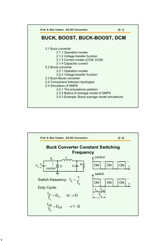
Design of DC-DC Converters Frank Xi fxi@monolithicpower.com - PowerPoint PPT Presentation
Design of DC-DC Converters Frank Xi fxi@monolithicpower.com Monolithic Power Systems Inc. IEEE SSCS Dallas Chapter, October 2007 Design of DC-DC Converters DC-DC Converter Basics Topology and Operation of DCDC Converters Control
Design of DC-DC Converters Frank Xi fxi@monolithicpower.com Monolithic Power Systems Inc. IEEE SSCS Dallas Chapter, October 2007
Design of DC-DC Converters � DC-DC Converter Basics � Topology and Operation of DCDC Converters � Control Scheme for DCDC � DC-DC Converter Design Techniques � System Level Modeling and Design � Building Block Design Considerations 11/1/2007 IEEE SSCS - Oct. 2007 2
DC-DC Converter Basics � DC-DC Converter is a Voltage Regulator � Use Switches, Inductor and Capacitor for Power Conversion � Switched Mode Operation � Why DC-DC Converters? � High Efficiency � Can Step-Down, Step-up, or Both, or Invert � Can Achieve Higher Output Power 11/1/2007 IEEE SSCS - Oct. 2007 3
DC-DC Converter Basics � Why not DC-DC Converters? � Complex Control Loop � Higher Noise and Output Ripple � More External Components � Basic DC-DC Converter Topologies � Majority of DC-DC uses PWM Control Operated in CCM Mode 11/1/2007 IEEE SSCS - Oct. 2007 4
DC-DC Converter Basics � Step-down (Buck) L Basic Relationships I O V IN V SW V OUT S I IN I L I D I C � CCM Mode D C � I L always supplies load � I C small, independent of V SW T load V OUT T T ON = = ⋅ I L ON V V D V OUT IN IN T I O = ⋅ I D I IN OUT I D I IN � DCM Mode Continuous Conduction Mode (CCM) I L 2 T = ON V V I O ⋅ ⋅ OUT 2 IN I L T 2 + O T ON V Discontinuous Conduction Mode (DCM) IN 11/1/2007 IEEE SSCS - Oct. 2007 5
DC-DC Converter Basics � Step-up (Boost) Basic Relationships L D I O V IN V SW V OUT I L � CCM Mode I C S C � I L only supplies load during T OFF period V SW T � I C large and load dependent V OUT T ON T OFF T 1 = = ⋅ I L V V V − OUT IN IN 1 T D OFF 1 I C = = ⋅ I I I − IN L OUT 1 D � DCM Mode -I O Continuous Conduction Mode (CCM) ⋅ ⋅ 2 I L I L T 2 + O T ON V I C = IN V V OUT IN 2 -I O T ON Discontinuous Conduction Mode (DCM) 11/1/2007 IEEE SSCS - Oct. 2007 6
Common Control Architectures � Modulation Scheme � PFM (Pulse-Frequency-Modulation) � Pulse Skipping, Hysteretic, Constant-on etc. � High Efficiency at Light Load � Inherently Higher Output Ripple � Unmanaged Spectrum Noise � PWM (Pulse-Width-Modulation) � Fixed Frequency with Variable Duty Cycle � Better Transient Response (except Hysteretic?) � Most Widely Used 11/1/2007 IEEE SSCS - Oct. 2007 7
Common Control Architectures � Control Method (for PWM) � Voltage Mode � Regulates Output Voltage by Adjusting Duty Cycle � Constant Ramp for Modulation, Better Noise Immunity � LC Filter Contributes to Complex Conjugate Poles � Loop Has No Information on Inductor Current � Slower Response to Input Voltage Change � Bandwidth Varies with Input Voltage � Current Limit Done Separately 11/1/2007 IEEE SSCS - Oct. 2007 8
Common Control Architectures � Current Mode � PCM (Peak-Current-Mode) Most Commonly Used � Regulates Inductor Current to Satisfy Load Demand and Maintain Output Voltage � Fast Current Loop makes Inductor to be a VCCS, eliminates Complex Conjugate Poles � Easy Built-in Cycle-to-Cycle Current Limit � Naturally Suitable for Multi-Phase Operation � Current Sense Susceptible to Noise � Need Slope Compensation for >50% Duty Cycle Operation 11/1/2007 IEEE SSCS - Oct. 2007 9
DC-DC Converter Design � Examples of Common DC-DC Converters � Voltage Mode Buck S1 L V IN V SW V OUT R 1 R ESR CLK R L S2 D’ V RAMP R 2 V EA C V SW V OUT D Q S CLK I L I OUT V RAMP V FB RST QB R V EA EA V REF 11/1/2007 IEEE SSCS - Oct. 2007 10
Voltage Mode Buck Voltage Mode Buck Transfer Functions: + + ( 1 ) ( 1 ) v sCR sCR ≈ = O ESR ESR V V IN IN 2 L s s d + + + 2 + + ( ) 1 s LC s CR 1 ESR ω ω 2 R Q L 0 0 1 1 ω = = , Q 0 1 LC L C + R ESR R C L L and 1 d = ( ) a s v V FB R where is the transfer function of the error amplifier ( ) a s 11/1/2007 IEEE SSCS - Oct. 2007 11
Voltage Mode Buck Control (Duty Cycle) to Output Transfer Function: Example: L=2.2uH, C=22uF, R ESR =10m Ohm V IN =5V, V OUT =3.3V R L =10 Ohm F SW =1.5MHz V RAMP =100mV ω 0 = 22.9kHz Q = ~15.8 ω Z = 700kHz 11/1/2007 IEEE SSCS - Oct. 2007 12
Voltage Mode Buck - Error Amp Ex. 1 Use low DC gain to set the bandwidth so that the phase margin is acceptable: R1 R2 V EA V FB Bandwidth: ~400kHz Phase margin: ~35° Conditionally stable EA V REF R = + − 2 ( ) V V V V EA REF REF FB R 1 R = − 2 v v EA FB R 1 + ( 1 ) R V sCR = − ⋅ 2 IN ESR LG 2 s s R V + + 1 R 1 ω ω 2 Q 0 0 Closed loop step response Example: R2=500k, R1=100k, V R =100mV 11/1/2007 IEEE SSCS - Oct. 2007 13
Voltage Mode Buck - Error Amp Ex. 1 Some Improvements Can Be Added: � Make V RAMP proportional to V IN -> Constant Bandwidth � Add Feed-forward Cap on Feedback Resistor String -> better phase margin Limitations of Low DC Gain: � Loose Output Regulation � Need some ESR to Stabilize the Loop � Small Modulation Ramp Sensitive to Noise � DC Offset if Output Cap has large ESR 11/1/2007 IEEE SSCS - Oct. 2007 14
Voltage Mode Buck - Error Amp Ex. 2 Use Type-III Compensation Network to Re-Shape Loop Frequency Response: Example Design Steps: 1. Set R 1 C 2 =100uS for desired C 3 C 2 R 2 BW of ~300kHz V FB 2. Set 1 st zero to be 1/5 of ω 0 : C 1 R 3 R 1 R 1 =1Meg, C 1 =30pF, ω z1 =5.3kHz EA V EA 3. Set 2nd zero to be 4x of V REF ω 0 : C 2 =10pF, R 3 =200k, + + + ( 1 )[ 1 ( ) ] ω z2 =79.5kHz v sC R s R R C ≈ − EA 1 1 3 2 2 A + + + + + 0 [ 1 ( 1 )( )]( 1 )( 1 || ) v sR A C C sR C sR C C FB 3 0 1 3 2 2 1 3 1 4. mid-band DC gain of 5: + + + ( 1 )( 1 ) ( 1 ) sC R sR C V sCR ≈ − ⋅ 1 1 3 2 IN ESR LG A R 3 =200k 0 + + + 2 [ 1 sR A C ]( 1 sR C )( 1 sR C ) V s s + + 3 0 1 2 2 1 3 R 1 ω ω 2 5. Set 2 nd and 3 rd pole to near Q 0 0 1 V ≈ ⋅ ⋅ IN UGBW R C switching frequency for 1 2 V LC R high frequency noise • High DC gain rolls off by dominant pole and, phase shift recovered by 1 st zero before ω 0 attenuation: • 2 nd zero brings back phase shift above ω 0 C 3 =0.2pF, ω p2 =795kHz; • 2 nd and 3 rd pole attenuates high frequency noise R 2 =10k, ω p3 =1.5MHz 11/1/2007 IEEE SSCS - Oct. 2007 15
Voltage Mode Buck - Error Amp Ex. 2 • Modulation ramp V RAMP increased to Compare to Error Amp Ex. 1: 500mV for better noise immunity • Step response has less overshoot • Blue: control to output transfer function due to better phase margin • Green: Type-III compensation error • Settling is much slower due to 1 st Amp transfer function zero at low frequency • Red: Complete loop transfer function bandwidth: ~340kHz, PM: ~65 degree 11/1/2007 IEEE SSCS - Oct. 2007 16
DC-DC Converter Design � Current Mode Buck (Peak Current Control) S1 L V IN V SW V OUT R 1 R ESR CLK R L S2 D’ V EA R 2 C V RAMP RST R SEN V SW V OUT Slope Comp D I L I OUT Q S CLK V RAMP RST V FB QB R V EA EA V REF 11/1/2007 IEEE SSCS - Oct. 2007 17
Current Mode Buck Inductor Current Instability for Duty Cycle > 50%: n ⎛− ⎞ m m ⎜ ⎟ + = ⋅ − = ⋅ 2 2 1. D=1/3: m 2 /m 1 =1/2 [ 1 ] [ ] ( ) [ 0 ] i n i n i ⎜ ⎟ e e e ⎝ ⎠ m m 1 1 i e [n] m m 1 < m 2 2 1 : attenuates over cycles i e i e [n+1] m 1 m 2. D=2/3: m 2 /m 1 =2 > 2 1 : grows over cycles i e m 1 i e [n] m 2 Requires Slope Compensation: m 1 i e [n+1] − m m + = ⋅ − 2 [ 1 ] [ ] ( a ) i n i n + e e m m 3. D=2/3 with slope compensation 1 a − m m < m a 2 is chosen so that a 1 m + a m m 1 a i e [n] m = 2 ex : , guaranteed stable m i e [n+1] a 2 = , 1 cycle correction m m 2 a 11/1/2007 IEEE SSCS - Oct. 2007 18
Current Mode Buck • Fast current loop regulates inductor peak current, can be modeled as a VCCS with output impedance Rx • Slower voltage loop provides reference for current loop 1 1 1 1 i = = = G o m R X R T m R v R R + + − − + 1 L S [( 1 a )( 1 D ) 0 . 5 ] 1 L EA SEN SEN L m R 1 X I O G m L V IN V OUT where = R X m + − − [( 1 a )( 1 ) 0 . 5 ] T D S m R 1 1 R ESR Switched Operation results in delay and sampling effect : + α − − − sT R L 1 1 e m m S = where α = ( ) 2 a H s − + α ⋅ + e sT 1 e sT m m S 1 S a R 2 C Complete VCCS transcondu ctance including frequency response : − + α − sT 1 1 1 1 e S = ( ) G s − m + α ⋅ R T m sT 1 R e sT + + − − S 1 L S [( 1 a )( 1 ) 0 . 5 ] D SEN S L m 1 1 1 1 ≈ G ( s ) V FB m 2 R s s R + + + 1 L V EA SEN 1 EA ω ω 2 R Q X S S V REF 2 1 2 1 = = Q π π m m + − − − − ( 1 a )( 1 ) 0 . 5 1 2 ( 1 a ) D D m m 1 2 11/1/2007 IEEE SSCS - Oct. 2007 19
Current Mode Buck Peak Current Mode Current Loop Transfer Function Example: L=2.2uH, V IN =5V, V OUT =3.3V, R L =10 Ohm R SEN = 0.5 Ohm F SW = 1.5MHz Blue: m a =0.5*m 2 R X =19.4 Ohm Gm=1.32 A/V Q=1.87 Green: m a =m 2 R X =6.6 Ohm Gm=0.80 A/V Q=0.64 11/1/2007 IEEE SSCS - Oct. 2007 20
Recommend
More recommend
Explore More Topics
Stay informed with curated content and fresh updates.

![Drivers Prof. S. Ben-Yaakov , DC-DC Converters [8- 2] Driving a MOSFET L D V in V o R L C 1](https://c.sambuz.com/1030065/drivers-s.webp)
![1 Prof. S. Ben-Yaakov , DC-DC Converters [8- 4] Gate Current V S 15V L D V in V o t V gs R g](https://c.sambuz.com/1030433/1-s.webp)
![1 Prof. S. Ben-Yaakov , DC-DC Converters [10- 4] Closed Loop V o Power v o stage R 1 - MOD](https://c.sambuz.com/839741/1-s.webp)


![1 Prof. S. Ben-Yaakov , DC-DC Converters [4- 4] Forward Converter L 1:n V o V in D 1 I L C I](https://c.sambuz.com/702678/1-s.webp)
