
SLIDE 1
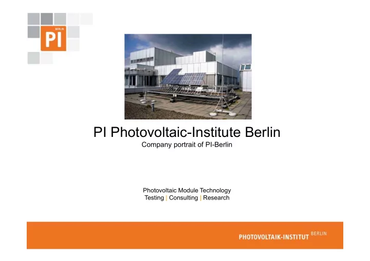
PI Photovoltaic-Institute Berlin
Company portrait of PI-Berlin
Photovoltaic Module Technology Testing | Consulting | Research
PI Photovoltaic-Institute Berlin Company portrait of PI-Berlin - - PowerPoint PPT Presentation
PI Photovoltaic-Institute Berlin Company portrait of PI-Berlin Photovoltaic Module Technology Testing | Consulting | Research At a glance Name: PI Photovoltaic-Institute Berlin (share holding company) Inscription: 10/12/2006 Investment: 1.2
Photovoltaic Module Technology Testing | Consulting | Research
Fig.1: Out-door measurement set-up in Berlin
23.4 m 7.7 m Laminator Load table Unlod table Climatic chamber 1 temperature cycling Climatic chamber 2 humidtiy- cold cycling Climatic chamber 3 humidity- heat cycling 2.8 m Steady
Simul. UV test
(→ Research → Service)
[Krauter &Grunow 21th PVSEC (2006), p.2065]
[Photon International 03/2006]
module eff. Tkoeff Pmax
coff FF NOCT a-Si (triple) 5.3%
0.11%/K
0.02%/K 45.1 a-Si (tandem) 5.2%
0.07%/K
0.03%/K 49.0 CdTe 7.7%
0.05%/K
0.02%/K 45.1 a-Si (single) 5.5%
0.09%/K
0.00%/K 47.7 DSC 0.8%
0.50%/K
40.0 HIT 15.1%
0.03%/K
49.0 mono Si 11.6%
0.05%/K
45.8 CIS 9.1%
0.04%/K
47.0 multi Si 11.8%
0.05%/K
45.0 multi EFG Si 11.6%
0.10%/K
46.3 Ribbon Si 10.0%
0.06%/K
44.0 mono LGBC 13.3%
0.05%/K
47.0 Apex 7.6%
0.08%/K
45.7
40% 50% 60% 70% 80% 90% 100% 0° 10° 20° 30° 40° 50° 60° 70° 80° 90° incident angle Isc/cos
Q6L Diamant Q6L Alberino T Q6L Alberino P
[Grunow et al. 20th EPVSEC (2005) p.2384]
[Grunow et al. 19th EPVSEC (2004), p.2190]
a-S i/µ
i a-S i/µ
i a-S i/µ
i a-S i/µ
i a-S i/µ
i a-S i/µ
i µ
i µ
i µ
i µ
i µ
i µ
i µ
i C dT e C dT e C dT e C dT e C dT e C dT e C IG S C I G S C IG S C IG S a-S i/a-G e a-S i/a-G e a-S i/a-G e a-S i/a-G e a-S i/a-G e a-S i/a-G e a-S i/a-G e a-S i/µ
i C dT e C I G S C IG S C IG S
0% 10% 20% 30%
direct AM 1.0 direct AM 2.0 direct AM 5.6 diffuse AM 1.0 diffuse AM 1.5 diffuse AM 2.0 diffuse AM 5.6 a-S i/µ
i µ
i C dT e C I G S a-S i/a-G e m ulti c-S i acidic m ulti c-S i m
i
[Krauter et al. 21th PVSEC (2006), p.2065]
[Herrmann, PERFORMANCE IP, ISPRA Workshop on Thin Film Module Technology 8./9. Nov 2006]
R&D; Testing, Consulting