
SLIDE 1
Special Topics in Optical Engineering II (15/1) 유병민
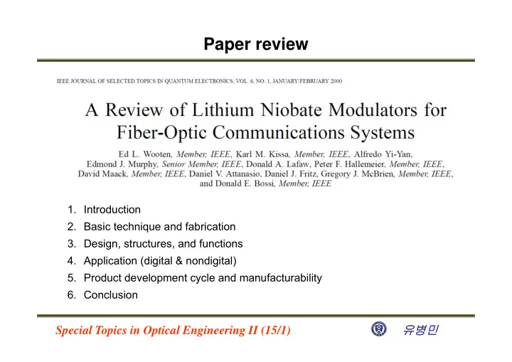
Paper review
- 1. Introduction
- 2. Basic technique and fabrication
- 3. Design, structures, and functions
- 4. Application (digital & nondigital)
- 5. Product development cycle and manufacturability
- 6. Conclusion