
SLIDE 1
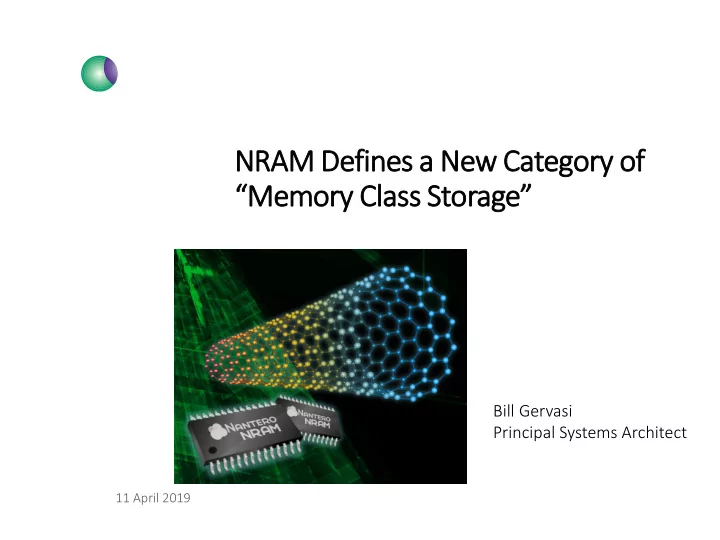
NRAM D Defines a a New C Categor gory o
- f
“Memory C Class S ss Storage”
11 April 2019
Bill Gervasi Principal Systems Architect
NRAM D Defines a a New C Categor gory o of Memory C Class S - - PowerPoint PPT Presentation
NRAM D Defines a a New C Categor gory o of Memory C Class S ss Storage Bill Gervasi Principal Systems Architect 11 April 2019 2 NR NRAM Technol ology ogy Value Te Test Propos osition on Results ts Age genda Marke
11 April 2019
Bill Gervasi Principal Systems Architect
2
3
4
NVDIMM NVMe
5
Run DRAM AM Run Run Run Run Run Run No Non-Volatile M e Memory SSD/HDD Chec eckpoint Run SSD/HDD Chec eckpoint Run SSD/HDD Chec eckpoint
6
…………….. …………….. ……………..
7
8
9
Nanotubes a are i in full p production t today Fundam amental al r resistan ance i is constan ant Leng ength a and nd d diameter er can b n be selec ected ed Mec echanically, t ther hermally, & elec ectrically s stable
10
Van d n der W Waals e ener ergy b barrier er keep eps C CNTs s apa part or together er Data reten ention > >10 0 years ( (more l e like e >1000 y 000 years) s) Stocha hastic a array of hundr ndreds ds nano notub ubes p per e each c cell
ELECTROD ODE ELECTROD ODE
11
TOP METAL BOTTOM ELECTRODE
SET: Void Shrinks above BE RESET: Void stretches above BE
F↑ + + F
12
13
13 cyc
14
Key f factor i is the he num number o
unctio ions ns pe per bi bit (>100 ne neede ded) Swi witching demonstrated f from 180n 180nm t to 15n 15nm Modeli ling s sho hows viabil bilit ity t to 1 1 nm nm l logic ic pr process
15 Substra rate
Logi gic/Memory p process
Cro rossover a aro round Hig igh M Mb or
Gb Function o
Desi sign E Efficien ency nR Crossp spoint
1T-1R m matr trix
nR Crossp spoint nR Crossp spoint nR Crossp spoint
1T 1T-1R m matr trix 1T-1R m matr trix 1T 1T-1R m matr trix
Ei Eith ther… Or Or Bo Both th
16
More like t tradit itio ional D l DRA RAM; be better f for s small ll arrays
1T-1R NRAM in Memory Process Wafer er / / C Circuits Dra rain Plate Dra rain Dra rain
17
0 1 2 3 H1<0> H2<0> H1<1> H2<1> V1<0> V2<0> V1<1> V2<1> V1<2> V2<2> V1<3> V2<3> V1<4> V2<4> V1<5> V2<5> V1<6> V2<6> V1<7> V2<7> H1<2> H2<2> H1<3> H2<3> 0 1 2 3 0 1 2 3 0 1 2 3 0 1 2 3 0 1 2 3 0 1 2 3 0 1 2 3 0 1 2 3 0 1 2 3 0 1 2 3 0 1 2 3 0 1 2 3 0 1 2 3 0 1 2 3 0 1 2 3 0 1 2 3 0 1 2 3 0 1 2 3 0 1 2 3 0 1 2 3 0 1 2 3 0 1 2 3 0 1 2 3 0 1 2 3 0 1 2 3 0 1 2 3 0 1 2 3 0 1 2 3 0 1 2 3 0 1 2 3 0 1 2 3
Cel ells c constructed ed from res esistive el elem ements between en l lines es Sel elf-selecting due due t to extremely ly low l leakage
V1 V1 V1 H2 H2 H1 V2
18
Drivers rs Recei eiver ers Z Y X
NRAM AM L LAYE YER
Tune t e the e array s size e to the e size e of d drivers & & rec eceivers Chi hip-level t tim iming i is a function o
line fli light tim imes Repl plicate t thi his “ “tile” as ne neede ded f for de device capa pacit ity Add I dd I/O dr drivers to emula ulate a any PH PHY ne neede ded
I/O PHY 64 Kb tile X 256 K tiles = 16 Gb
19
HBM BM HMC DDR DR4/ 4/DDR DDR5 LPDDR DDR GDDR DR eRAM AM Cust stom
20
A0:16 BG0:1 BA0:1 PAR C0:2 CMD CK DQ0:3 LDQS DQ4:7 UDQS 3DS DS stackabl ble
21
Data Strobe Data Strobe FIFO FO FIFO FO SEC ECDED ED EC ECC Engi gine 64 bits 72 bits x4/x /x8 Address Ro Row Decode de Colu
Decode de Carbon N n Nanotube ube A Arrays Chip ID Die S e Selec ector Bank Decode de
22
Latchi hing S Sens nse A Amp Shadow B Buffer er CNT A Arra rray
ACTI TIVATE TE trans nsfers d data fro rom a arra ray to sense a nse amps Background und shadow b buffers allo llow c com
to N
V array READs Ds a and WRITEs f flow throug ugh s h sense a amps ps WRITE DATA ATA CNT NT tPERS
RSIST = 4
46.25 n 25 ns Shadow c copy
Lo Loads LS LSA fro rom C CNT Updates L LSA SA with h ex ext data ta
External Internal
tRCD
CD
tAA
AA
AC ACT Vs DDR s DDR4, Slig lightly ly l longer tRCD
CD,
signif ific icantly s shor
AA
23
Para rameter NRAM4 M4-2666 2666 DDR DR4-2666 2666-D 3DS 3DS
tRC RCD
RAS AS t to C CAS AS
23. 23.0 15. 15.0 18. 18.18 18 tRP RP
Precharg rge
14. 14.25 25 15. 15.0 18. 18.18 18 tRAS
Activate t e to prechar arge
32. 32.0 32. 32.0 32. 32.0 tWR WR
Write r recovery
23. 23.0 15. 15.0 45. 45.0 tFA FAW
Fou
activate w win indow l lim imit it
21. 21.0 21. 21.0 tRFC FC
Refresh esh t time
550 550 295 295 _L _L / / _S _S
Bank g k grou
to b bank g k grou
No pe pena nalty _S S Slower _S S Slower
DDR DR5-4400C 4400C
tRC RC
Activate t e to a activate
46. 46.25 25 47. 47.00 00 50. 50.18 18 tAA
Rea ead t to d
13. 13.5 17. 17.14 14 18. 18.18 18 3D 3DS
Chip t to chip i in stack
No pe pena nalty 2ck pe pena nalty 4ck pe pena nalty
Latency: smaller is better
24
DDR4/DDR5 Elimination o
efresh sh Elim limination of
FAW restrictions Elimina nation o n of bank g group p restrictions ns Elimination o
er s states es Base t throug ughp hput ut Archi hitec ectural i impr provem ements improve ve data t throug ughput hput 15 15% o % or grea eater er at t the s he same clock f freque uenc ncy 15-20% Bandwidth: larger is better Elim limination of
inter-die d e delays NRAM
25
16 16 Gb 28 28 nm l log
ic 4 4 layers rs C CNT 64 64 Gb 14 14 nm l log
ic 4 4 layers rs C CNT 128 Gb 128 Gb 14 nm l log
ic 8 8 layers C s CNT 256 Gb 256 Gb 7 nm l log
ic 4 4 layers C s CNT 512 Gb 512 Gb 7 nm l log
ic 8 8 layers C s CNT 8 8 Gb 28 28 nm l log
ic 2 2 layers rs C CNT New process Add layers New process Add layers DDR DR4 DDR DR5 8-di die s e stacks 16 16-di die s e stacks ~100 mm2 Add layers
26
DDR5 5 bus s is s limited to 16H 16H x 32Gb 32Gb = 8H 8H x 64Gb 64Gb NRAM lik ikely to s scale to a at least 256Gb/die in in DDR5 t tim imeframe We ne need t d to correct thi his restric ictio ion n in n JEDEC A qui quick pe peek a at DDR5 pr protocol r l reveals a a di dirty little le secret…
27
Na Nantero i is chair o
the J e JEDEC No Non-Vol
ile M Memor
Com
REXT XT ACTI TIVATE TE READ AD/WRITE TE
12 extend nded r d row bi bits ena nabl ble up up to 128Tb/ b/die die Developi ping ng DDR5 5 NVRAM S Spe pecific icatio ion
28 Magn gneti tic R RAM
Hard rd D Disk SSD NVMe DDR DR DRAM AM Wastel eland Resi sistive R e RAM 3D D Xpoint Flash sh
> DRAM p performa mance = DRA RAM e endu ndurance > DRA RAM c capa pacity < DRA RAM pr price
Phase C se Change
Fut Future SCM NRAM
3D N 3D NOR
Storage Storage C e Class Mem emory
29
Batter eries es & & Supe uperCaps are t e the e en enem emy t to be e defea eated ed Carbon na nano notube bes attract or repel l electrostaticall lly Mem emory cel ell performance = e = 5 5ns with no h no wear-out ut
temperatur ure issues es NRA RAM de define nes a ne new c category: Mem emory Class Storage Mem emory cel ells arranged in in til iles can n emula ulate a any standa dard i d interface Device c capa pacit ity roadm dmaps ps f for NR NRAM e exceed ed DRAM