mem o ry noun \memr, mem\ 1 a: the power or process of reproducing - PowerPoint PPT Presentation
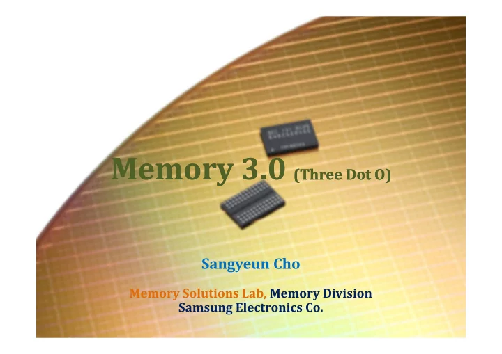
Memory 3.0 (Three Dot O) Memory 3.0 (Three Dot O) Sangyeun Cho Memory Solutions Lab, Memory Division Samsung Electronics Co. Memory 3.0 1 mem o ry noun \memr, mem\ 1 a: the power or process of reproducing or recalling what
Memory 3.0 (Three Dot O) Memory 3.0 (Three Dot O) Sangyeun Cho Memory Solutions Lab, Memory Division Samsung Electronics Co. Memory 3.0 1
mem o ry noun \ˈmem‐rē, ˈme‐mə‐\ 1 a: the power or process of reproducing or recalling what has been learned and retained especially through associative mechanisms … 4 a: a device (as a chip) or a component of a device in which information especially for a computer can be inserted and stored and from which it may be extracted when wanted Memory 3.0 2
mem o ry 1.0 2.0 (194x~1970) 3.0 Delay line (1949) (1970~) Drum memory (1953) Williams tube (1946) DRAM (1970) Core memory (1951) ??? SRAM Hard drives (1956) Flash memory (1988, 1992) Tape (1952) Hard drives Memory 3.0 3
4 1.0 Memory 3.0 mem o ry
Delay line (1949) • Sonic waves are injected at one end – These waves propagate through the media inside the “line” • Waves are retrieved at the [For UNIVAC I, 1951] other end and re-injected – States are preserved – New values can be injected 1 0 0 1 instead of old values • 100’s of bits • 100’s sec access latency • Address interleaving Memory 3.0 5
Drum memory (1953) • Rotating drum (metal cylinder) • Many heads (fixed) – (Random) access time of milliseconds • <100KiB • Non-volatile • Rotational speed determines performance [For ZAM-41, 1961] • Address interleaving In BSD Unix, /dev/drum is • Similar to the soon available the name of the default swap hard drive technology device Memory 3.0 6
Atanasoff-Berry Computer (1942) Each rotating drum has 1,600 capacitors, refreshed or updated every second [“ABC” @Iowa State University] Memory 3.0 7
Core memory (1951) [For Whirlwind, 1951] Read is destructive… Need to reprogram after each read Memory 3.0 8
Core memory (1951) • High density – $1 per bit $0.01 per bit • High performance – 1MHz clock rate • Non-volatile – This property was utilized in some In many systems, a dump of systems memory contents (after system crash) is called “core dump” Memory 3.0 9
First hard drive (1956) 50 platters @1,200rpm Avg. seek time ~600ms Data transfer rate ~9KiB/s $11,364 per MB Capacity < 5MiB Weight > 1 ton ~42 bits per gram [IBM RAMAC, 1956] Memory 3.0 10
Summary of mem o ry 1.0 • Introduction of familiar concepts like: – Sequential access vs. random access – Address interleaving – Retention vs. refreshing – Destructive reading • Births and deployment of lasting (or recurring) memory technologies like: – Hard drives – Tapes – Magnetic RAM – Capacitive storage ( DRAM) Memory 3.0 11
12 mem o ry 2.0 Memory 3.0
DRAM [Cha, 2011 VLSI Tech. Short Course] Memory 3.0 13
[Cha, 2011 VLSI Tech. Short Course] 14 Memory 3.0 DRAM scaling
NAND flash Dr. Fujio Masaoka @Toshiba 1980 invents flash memory in 1980 Intel produces first NOR flash 1988 in 1988 Toshiba introduces 4Mb NAND 1992 flash in 1992 Samsung develops 16Mb NAND 1994 flash in 1994 Memory 3.0 15
Hard drives WD Se 4TB SATA drive (2013) 7,200 RPM 64MB buffer Seek (avg.): several ms 4TB 0.75kg Memory 3.0 16
Hard drives, then and now RAMAC (1956) WD Se (2013) Ratio 60 2.5 1/24 Inch 5MiB 4TiB 800k Capacity >1 ton 0.75 kg 1/1,333 Weight 1,200 rpm 7,200 rpm 6 Rotation speed 600ms <5ms 1/120 Avg. seek 42 43B >1B Bits per gram ~9KiB/s ~100MiB/s 11.1k Bandwidth 9.25 min 667 min 72 Time to read out Time to read out 21 min 35 days 2,413 (4KiB random) Memory 3.0 17
Solid-state drives Flash Channel #0 Flash CPU On-Chip ECC On-Chip Host Interface Memory CPUs (s) SRAM SRAM … Controller Controller Host … … Flash Channel #( n ch –1) Flash DRAM ECC Memory Controller … Controller DRAM DRAM NAND Flash Array Memory 3.0 18
SSD market forecast SSD Shipment Avg. GB/Application GB Shipment 47% 45% 42% 35% 28% 21% [Source: IDC May 2013] Samsung: #1 SSD provider since 2007 Memory 3.0 19
Hard drive vs. SSD WD Se 4TB Samsung 841 Ratio 2.5 ‐ ‐ Inch 4TiB 512GiB 1/8 Capacity 0.75 kg 0.01 kG 1/75 Weight 7,200 rpm ‐ ‐ Rotation speed <5ms (negligible) ‐ Avg. seek 43B 410B 9.5 Bits per gram ~100MiB/s ~540MiB/s 5.4 Bandwidth 667 min 16 min 1/42 Time to read out Time to read out 35 days 22 min 1/2,291 (4KiB random) Memory 3.0 20
Summary of mem o ry 2.0 • Scaling rules! – DRAM has the crown in main memory (DDRx) – Hard drive capacity follows exponential growth curve • But… the performance of hard drives is stagnant – NAND flash memory starts to replace (high-end) hard drives and enable mobile revolution! – Flash is new hard drive, hard drive is new tape • However, … – Further, economic (planar) scaling is seriously questioned – Physical limitations (e.g., cell interference) are becoming (seemingly) harder to overcome Memory 3.0 21
22 mem o ry 3.0 Memory 3.0
NAND flash scaling trend 120nm 1Gb Cost of Patterning 90nm 2Gb 70nm 4Gb 60nm 8Gb 50nm 16Gb 40nm 32Gb 19nm 128Gb Memory 3.0 23
The era of mem o ry 3.0 • Economic planar scaling is *very* hard – It’s time to start planning for the end of Moore’s Law , August 2013, Bob Colwell (DARPA) – The end of Moore’s Law may ultimately be as much about economics as physics • We need creative approaches to scaling and adding value to memory solutions • Consider potentially more scalable memory technologies, e.g., resistive memories • As data-intensive applications and data locality become increasingly important, active or smart memory subsystems make more sense Memory 3.0 24
1. Device and technology innovations will continue (but for how long?) 40 35 30 half pitch (nm) 25 20 15 DRAM flash 10 5 [ITRS 2011] 0 2011 2012 2013 2014 2015 2016 2017 2018 2019 2020 2021 2022 2023 2024 2025 2026 Memory 3.0 25
128Gb V-NAND [Elliott and Jung, Flash Memory Summit 2013] “The World’s 1st 3D V-NAND Flash Mass Production” Comparing with 20nm planar NAND Flash • 2X Density and Write Speed • ½ Power Consumption • 10X Endurance 128Gb V-NAND Flash 24 Layer Cell Structure Memory 3.0 26
27 [JSSC 2010] Memory 3.0
2. New memories are coming? [Cryder and Kim, Trans. Magnetics 2009] Memory 3.0 28
Interest grows US Patents Granted PRAM MRAM FRAM (Lam, VLSI-TSA ’08) Memory 3.0 29
Samsung Techinsights decap ’10 Techinsights decap ’10 Techinsights decap ’10 Chung et al. ISSCC ’11 Lee et al. ISSCC ’07 Lee et al. JSSC ’08 1Gb @58nm 512Mb @90nm 512Mb @60nm? 512Mb @60nm? LPDDR2-N Diode switch design Diode switch design Diode switch design “Write skewing” 266MB/s read Believed to be a tech.- Believed to be a tech.- 6.4MB/s write 4.64MB/s write (x16) migrated design migrated design “DCWI” (~Flip-N-Write) Memory 3.0 30
Numonyx (now Micron) Numerous press releases (2011~2012?) Early access program (slated for MP in 2011) (2009) (www.micron.com) (Servalli, IEDM ’09) “Imola” and “Mandello” “Alverstone” (OMNEO) “Bonelli” 2Gb & 4Gb @45nm 128Mb @90nm 1Gb @45nm TR switch design 1.2V & 1.8V I/O 40MB/s read (?) 1.8V I/O LPDDR2-NVM & <1MB/s write (?) DDR3-NVM Memory 3.0 31
3. Closer and faster, please! [Keckler et al., IEEE Micro 2009] Memory 3.0 32
Distance of data sorely felt [Keckler et al., IEEE Micro 2009] 2010 2017 Process technology 40nm 10nm, high freq. 10nm, low volt. V DD (nominal) 0.9 V 0.75 V 0.65 V Frequency target 1.6 GHz 2.5 GHz 2 GHz Double ‐ precision FMA energy 50 pJ 8.7 pJ 6.5 pJ 64 ‐ bit read from an 8KiB SRAM 14 pJ 2.4 pJ 1.8 pJ Wire energy (256 bits, 10mm) 310 pJ 200 pJ 150 pJ Operand fetch from DRAM More than 10nJ Exascale goal: 20 pJ per floating point operation Memory 3.0 33
nVIDIA Echelon Want: 50 Gbps/pin @4.5pJ/bit Silicon interposer or MCM [Keckler et al., IEEE Micro 2009] Memory 3.0 34
HP Lab Nanostore [Ranganathan, IEEE Computer 2011] Memory 3.0 35
“Intelligent” SSD (iSSD) Flash Channel #0 CPU Flash On-Chip ECC On-Chip Host Interface Memory CPUs (s) SRAM SRAM … Controller Controller Host … … Embedded Scratchpad DMA Processor SRAM Flash Channel #( n ch –1) Flash DRAM ECC Memory Controller … Controller Bus Stream Flash Bridge Processor Interface Main Config. Controller Memory DRAM DRAM NAND Flash Array zero 0 zero N-1 … R 0,0 ALU 0 enable … … ALU N-1 result R 0,0 R N-1,1 ALU 0 zero ALU 0 … R 0,1 ALU N-1 … R 0,0 ALU 0 enable … … ALU N-1 result R N-1,0 R N-1,1 ALU N-1 zero ALU 0 … R N-1,1 ALU N-1 Scratchpad SRAM Interface [Cho et al., ICS 2013] Memory 3.0 36
Energy (energy per byte) 12 12 12 40 200 SSD I/O 30 NAND Energy Per Byte (nJ/B) 150 8 8 8 I/O DRAM 20 chipset 100 4 4 4 10 main memory SP 50 processor 0 0 0 0 host CPU 0 host ISSD ISSD w/ host ISSD ISSD w/ host ISSD ISSD w/ host ISSD ISSD w/ w/o SP SP w/o SP SP w/o SP SP w/o SP SP linear_reg. string_match k-means scan Legend • iSSD energy benefits are large! – At least 5× (k-means) and the average is 9+× Memory 3.0 37
4. Cooler and larger, please! [Nellans, Flash Memory Summit 2011] Memory 3.0 38
Recommend
More recommend
Explore More Topics
Stay informed with curated content and fresh updates.





![DNSSEC update TF MNM, Lyon Roland van Rijswijk roland.vanrijswijk [at] surfnet.nl February 16 th](https://c.sambuz.com/271550/dnssec-update-s.webp)
