
SLIDE 1
LumiCal Design Options
2020.04.15 15:00 indico.ihep.ac.cn/event/11684/
Suen Hou Academia Sinica
LumiCal Design Options 2020.04.15 15:00 - - PowerPoint PPT Presentation
LumiCal Design Options 2020.04.15 15:00 indico.ihep.ac.cn/event/11684/ Suen Hou Academia Sinica Outline BHLUMI : Bhabha cross section boost by beam crossing, small beam pipe < 30 mRad ( Bhabha) > ~ 50 nb OVAL beampipe to
2020.04.15 15:00 indico.ihep.ac.cn/event/11684/
Suen Hou Academia Sinica
2
3
Reference to Z-lineshape, e+e− → Z → qq ‾ Luminosity of e+e− collisions by measuring Bhabha elastics scattering
– QED process, theoretical < 0.1% precision – triggering on a pair of scattered e+e- σ = 41 nb
LO diagrams
Fiducial region
detector spatial resolution
4
LumiCal at z = ±1 m, θmin = 30 mRad δθ = 15 μRad or dr = 15 μm Error due to offset on Z 0.1 mm on z or dr = δ Rxθ = 3 μm
Bhabha θ-angle distribution
θmin
5
RIGH LEFT T
RIGHT
LEFT
Event signature
~1% events
6
7
Bhlumi 4.04 writeup: CERN-TH/96-158 cds.cern.ch/record/310621/files/th-96-158.ps.gz
http://cern.ch/~jadach/public/Bhlumi-linux-4.04-export_2002.11.05.tar.gz
Theory uncertainty: 0.25% was BHLUMI 2, reported in CPC package paper http://inspirehep.net/record/321226?ln=en The latest BHLUMI 4 report is pushed to < 0.1%
8
Xcru calculated for Thmin=0.7xTh1 to 2xTh2
count events in chosen condition scale to Xcru
9
Bhlumi-linux-4.04-export_2002.11.05.tar.gz Compiled by g77 on SL6, demo.f produce numbers as in paper CERN-TH/96-158
LEP workshop95 on Bhabha established 0.1% precision Hep-ph/9602393
de demo mo.f .f 10 1000 00000 000 ev ev KeyPia=0, KeyZet=0 CM CMS S = 9 = 92.3 2.3 GeV GeV Xsec_BARE1 = 162.5295 Nanob. Error = 0.2061 Nanob. Hep-ph/9602393
10
Beam crossing 33 mRad
11
Bhabha at detector plane Z=1m Opening angle –pi of scatterede+ e-
12
CMS generated th1=10 mRad boosted +16.5mRad, +X are low angle Bhabha Assuming beam pipe is LAB z-axis centered, radius = 30 mRad (r=30mm @z=1m) at x=+30 mm, Bhabha electrons are of θ=13.5 mRad Off beam pipe, detect: one electron (262 nb) / both electrons (74.6 nb) = 3.51 Hori. cut +/- 30mm :
Hits of ONE Bhabha electrons Hits of electrons, both detected
13
CMS 10 ~ 80 mRad
LAB detect ONE electron LAB detect both electrons
BARE1
full phi coverage
cut off ±30mm
full phi coverage
cut off ±30 mm
Nevents 457232 102535 20277 29194 19216 Xsec (nb) 1168.3
262.0
51.81
CMS 10 ~ 80 mRad
LAB ONE electron LAB both electrons
BARE1
full phi coverage
cut off ±30mm
full phi covearge
cut off ±30mm
Nevents 457232
135842 24236 34847 23010
Xsec (nb) 1168.3
61.93
Beam crossing: 33 mRad
Boost off ring center (+x axis) offset 16.5 mRad maximum (electrons on x-z plane)
Very hot region, Low angle Bhabha boosted outward LOW angle Bhabha on x-axis
the other electron (-x side) is boosted into beampipe NOT counted for Lumi meassurment
Far Forward Tagger on outgoing pipe trigger/back-to-back of low angle electrons < 50 mRad on x-axis lost into beam pipe
15
1st impact Si-wafer <5 um
Beam pipe flange
17
lateral shower spectrum agree with data
no upstream material
best spatial resolution
Arccos(0.99) (30~100)mrad (20~80)mrad 亮度探测器位置 顶点探测器位置
内铍管厚度: 0.50 外皮管厚度: 0.35 内外铍管间隙: 0.5 冷却介质:1号电火花油 说明: 1.Ø25和Ø31是根据白莎的计算,最小束流管孔径 2.亮度探测器对应管道为单层管(无冷却), 需根据计算确定184mm 是否满足温度要求
Ji Quan 18
Impact position is not effected by multiple scattering/fragmentation
50 GeV electron, shoot LumCal center theta = 40 mRad
1 mm 20 μm 1 μm 19
GEANT simulation precision is 0.1 MeV
20
Flange has NO Tungsten layers
1st layer behind BeamPipe face of 5mm Cu
Flange has 1X0 2 Tungsten layers 21
Three Si layers at Z>670 mm NO Tungsten layers Spatial resolution ~ 20 μm Front 2 Si-layers of Q-pole LumiCal Pileup of shower ~1 mm resolution Position(Hits) – Electron projected 1st Si layer behind Beampipe cone at Z=515 mm Hit deviation better than 1 μm 22
Three Si layers at Z>670 mm Two 1X0 Tungsten layers behind Si wafers Spatial resolution ~ 20 μm Front 2 Si-layers of Q-pole LumiCal Pileup of shower ~1 mm resolution Position(Hits) – Electron projected 1st Si layer behind Beampipe cone at Z=515 mm Hit deviation better than 1 μm 23
24
Assuming a tube beam-pipe joint of Be, Cu Electron Traversing 2mm Cu pipe very “THICK” in forward direction
25
At Z=50cm passing 1mm Cu ~ 1X0 material
Radiation length http://pdg.lbl.gov/2014/AtomicNuclearProperties/ X0(Be) = 35.28cm X0(Al) = 8.90 cm X0(Si) = 9.37 cm X0(Fe) = 1.76 cm X0(Cu) = 1.44 cm X0(W) = 0.35 cm
OuBP outer Be pipe Z=0~115 mm inner radius 28/2+1 mm 0.35mm thick
401 InBPipe
InBP Inner Be pipe Z=0~118 mm, inner diameter 28 mm 0.5mm thick 14 mm 15 mm 100 mrad
acos(.99) = 141.54 mRad @Z=118 r= 16.81 (=tanQ*118) acos(.992)= 126.58 mRad @Z=118 r= 15.02 mm Q= 100mRad @Z=118 r= 11.84 mm @Z=153 r=15.35 mm
Fpip flange pipe 1.5 mm thick Z= 522-716 mm at Z=512 r= 14 – 15.5 mm Fend Flange 20mm Z=696 - 716 r= 15.5~123.2 mm 409 TbFe 5mm Fe Z=0~ 970 mm connecting to r= 12.34cm ~+.5cm, FE Z=520 mm Z=115 mm Z=118 mm InAl Inner Al pipe Z=118~500 mm, inner diameter 28 mm 0.5mm thick OuAl outer Al pipe Z=0~115 mm inner r=28/2+1 mm, 0.35 mm thick Acos(.99) = .14154 rad Acos(.992) = .1266 rad atan(123.6/970) = .12678 rad
Acos(.992) =.1266 rad
Flng 10mm thick flange Z=520~530 mm r= 55~123.2 mm Fwin window 2 mm Z=520~522 r= 15.35~55 mm
TbIS 2mm scin Z=0~ 970 mm r= 12.32cm +.2cm TbOS 2mm scin Z=0~ 970 mm r= 12.39cm +.2cm
419 FLSi Si deck Z=522~524 R = 15.5-55. mm 29.7-105 mrad
SiW edge atan(70/685) =.1018 rad
FS0i SiW two layers Deck=3.5mmW+2mmAir R = 15.5-70. mm 22.3-100.2 mrad @ Z= 696
BpSn Si octagon rmin =1.5451 cm Z=16 - 52.0 cm
Al dual tubes .5mm, .35 mm thick
Flange has NO Tungsten layers
Flange front layer
Flange has two 1X0 Tungsten layers 28
Octagon Si wafers
Three Si layers at Z>670 mm NO Tungsten layers Front 2 Si-layers of Q-pole LumiCal Pileup of shower ~1 mm resolution Position(Hits) – Electron shower 1st Si layer behind flange at Z=515 mm 29 Octagon Si layers surrounding beampipe
Front 2 Si-layers of Q-pole LumiCal Pileup of shower ~1 mm resolution Position(Hits) – Electron shower 1st Si layer behind flange at Z=515 mm 30 Octagon Si layers surrounding beampipe
Three Si layers at Z>670 mm Two 1X0 Tungsten layers between Si wafers
31
δL/L ~ 0.01 %
IP σ<100 μm Diamond rings for calibration Fine segmentation of BGO crystal Use diamond Ring edges To calibrate Strip edge To calibrate
32
at z=50 cm, θ= 30 mRad δθ = .75 μRad or dr = .75 μm scaling to dz by 1/tan(.030)= 33 dz = 25 μm Si strip, pitch in Z, 300 μm thick traversing distance in z = 10 mm Si wafer coverage (30-100 mRad) z range 150 – 500 mm Assuming Si strip pitch = 100 μm (fire 100 strips @ 30mRad) resolution is determined by the fraction of entrance strip (low z) Optimized the pitch vs the 25 um resolution requirement and resolution distraction for the error on mean
IP σ<100 μm Octagon Si-strip in z LYSO + SiPM 2x2 mm2 strips Si strip disks In Flange Octagon Si-wafers surrounding beampipe Radius 15 mm
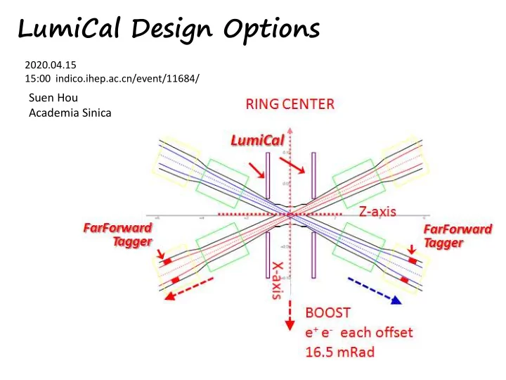
Boost due to 33mRad beam crossing
Symmetric to out-going beam-pipe, NOT the LAB frame
Lab z-axis
LumiCal LumiCal Far forward tagger Far forward tagger
Luminosity, Bhabha 測量條件:
LumiCal challenge:
-x 方向 electron 被推進 beampipe, 截面 減少 1/3 Bhabha 截面 > 41 nb 有困難
LumiCal 設計限制
沒有材料阻檔,最乾淨的 Bhabha 不能放Calo, 會導致 shower background to tracker
full Calo, 量 electron Ebeam, Bhabha Theta 模糊
beam monitoring, 測量小角度 Bhabha, 閃鑠體,包覆約2cm厚 2~5cm長,phi 細分割,標定 beam electron 在前端單管時, -x 方向被boost 進 beampipe Bhabha,分管後能被 trigger 以 back-to-back coincident,另一端“single electron Bhabha”是精密測量到的 這些 Bbabha ,是 33mRad 丟失掉的 1/3事例截面
Recover “Single Electron Bhabha” with Far-forward LumiMonitor
RING CENTER Z-axis BOOST e+ e- each offset 16.5 mRad
FarForward Tagger FarForward Tagger
LumiCal