
SLIDE 1
LEP400 Etch Depth Monitor Real-time, in-situ plasma etch depth - - PowerPoint PPT Presentation
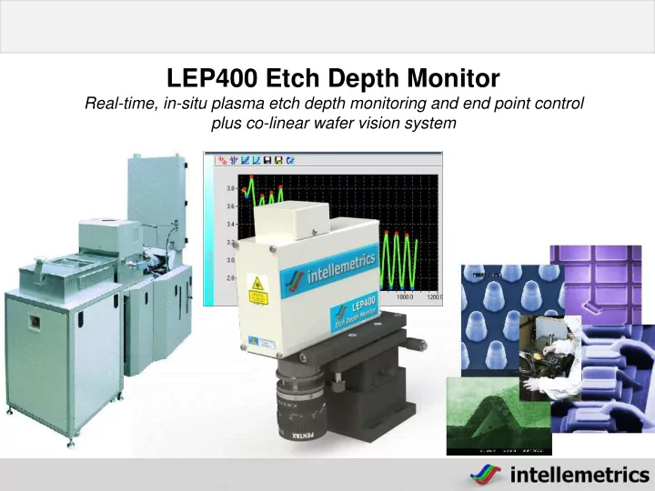
LEP400 Etch Depth Monitor Real-time, in-situ plasma etch depth monitoring and end point control plus co-linear wafer vision system Base Configuration Etch Depth Monitoring LEP400 Recessed Window Laser Spot on Plasma Plasma Patterned Wafer
Etch Depth Monitoring Laser Spot on Patterned Wafer
Surface Layer Removal Bulk Material Etching Signals from etching surface and bottom of wafer Bulk Material Etching Signals from mask and etching surface of wafer Wafer Stack Etching Signals from etching surface and every other interface of wafer stack
Transparent Opaque
Monitoring InP at 670nm Fringes seen only when layer is thin
~ 700nm
Monitoring InP at 980nm Clear fringes throughout Figure of Merit Maximum Measurable Thickness for Different Materials & Wavelengths Wavelength Material Max Depth Measureable 670nm SiO2, SiN, GaN, AlO2 GaAs InP Effectively infinite ~ 2,000nm ~ 700nm 980nm Most III-Vs Silicon Effectively infinite ~ 2,000nm If in doubt…we simply model the performance.
ECR
Optoelectronics
Lasers / Modulators / Detectors
Silicon Electronics
CMOS, trench isolation, wafer thinning, via holes
MEMS
Vapour release etch, deep silicon etch
III-V Electronics
HEMTs, HBTs
Photomask
Metal etch
Packaging
Topographic surfaces
Bio-Chips
Micro-channels
Failure Analysis II-VI Silicon Dielectrics Polymers Metals III-V Vapour Etch ICP RIE
LEP400 Head / Mount LEP400 PC-Based Controller Wafer Vision System
(B&W monitor or capture card)
Signal Level Meter for easy visual setup Data Logging info Intuitive control buttons. These enable the user to put the system into automatic control mode, or to manually take control of the etch process. In MANUAL MODE the user presses these buttons to take full control. In AUTOMATIC MODE these buttons are controlled via digital IO from the plasma etch system. Status LEDs
Process info
Etch time Signal Level Etch Rate Etch Depth
> 250 Materials Supplied as standard for 670nm unit including n, k values User can add hundreds more custom layers Databases available at 670nm, 860nm, 980nm, 1500nm and 1550nm User can create databases at other wavelengths as required
Input Materials directly from Material Database or custom user input Layer thicknesses in mm, nm or Å Rapid input for repeated quantum-well structures Number of layers: 1 to many hundreds
Graphical Visualisation Signal vs Etch Depth in mm, nm or Å Turning point markers On / Off Zoom Modes Pan Drag Window Zoom All Save Modes .mod BMP CSV
Resist Silicon
Does not require layer thickness to be known! Proven to detect the interface well before a skilled human operator!
Ideal for endpointing during metal etch
Hunts for a threshold in slope. Can be set to endpoint anywhere down the slope. Hunts for a ‘flatline’. Can be set to endpoint anywhere on the ‘cusp’ or into the flatline region. Ideal for endpointing on an etch stop.
Reads in saved RAW data in Real Time to simulate an etch run Data from: A previous run Standard sine wave (plus programmable noise) Enables runs to be simulated OFFLINE with different endpoint analysis modes, filter settings, hold-off, over-etch, etc Test your process will hit the required endpoint every time Ideal for rapid process optimisation on a desktop computer
Simulated run showing: Filtered data Turning point fitting
Automatic Data Logging of each run Raw data Filter settings Endpoint parameters User Specified Directories Filename Formats Includes run number sequence number date and time stamping Automatic data logging of all Control Panel status changes
Digital I/O provided as standard for integration of LEP400 into a customer’s etch tool 8 TTL I/O Lines on a 25 way socket Fully configurable via DIGIO Client software within EtchDirector Further I/O available on request Automatic search and recognition of a range of digital IO PCI cards Mutliple cards of the same or mixed type can be used Automatic search and recognition of the appropriate drivers Establishes the following virtual status outputs Idling / WaitingForGo / Etching / OverEtching / InterCutting / Cutting / Holding Establishes the following input command inputs Start / Go / ForceCut / Hold / Continue Any physical digital input on any card can be mapped to any virtual input or any number of virtual inputs. Any physical digital output on any card can be mapped to any virtual output or number of outputs Runs as a free standing executable with its own GUI which simplifies setting up of the digital IO Provides push buttons to override inputs and outputs Provides LEDs to show status of inputs and outputs Provides a log to record in/out activity The physical characteristics of the ports can be edited on a port by port basis. direction …input or output (if supported by card) sense… inverted or normal edge or level triggered if an input pulse or fixed if an output qualification period presetable for inputs pulse period presetable for outputs
Courtesy of Dr Geoff Hill, Sheffield University, UK
EtchDirector detects the 'flat-line' at the end of the oxide etch avoiding unwanted removal, damage or contamination of the underlying Al layer. A major advantage of this algorithm is that reliable endpointing does not depend upon the starting oxide thickness. This is especially important in a manufacturing environment where premeasurement of the oxide thickness is prohibitive in terms of time and cost. Ideal for monitoring the etch of SiN on metal or even combinations of SiN on SiO2 or on Si.
EtchDirector comes with an endpoint algorithm specifically designed to identify this step level change and enables the operator to choose whether to stop at the top, middle or bottom of the curve. Again, an
A major advantage of this algorithm is that reliable endpointing does not depend upon the starting metal
thickness is prohibitive in terms of time and cost. This process works even at high etch rates and has been proven to be faster and more accurate than a skilled operator. The process works equally well for other metals including NiCr, Ni, Au, Tg, Pt, etc, and works for a wide range of substrates.
Metals are not transparent until very thin and therefore you cannot
interference fringes and monitor etch depth & rate through the bulk of a metal layer. However, the LEP400 is ideal for picking
change in reflectivity.
Selective low damage plasma etch processes are used in a number of applications including III-V etching of InP & GaAs HEMTs and for active III-V
modulators and detectors. Often these processes experience an induction period at the beginning of the etch process during which the native oxide, and/or residues from the previous process stage, inhibit the etch. Once this layer has been removed the etch proceeds as normal. The problem is that the induction time is variable and may become a significant proportion of the expected etch duration. Without in-situ monitoring this can lead to large uncertainties in the etch depth. The LEP400 enables the operator to actually 'see' the induction period, as shown in the graph above, and still obtain a highly accurate and repeatable etch process.