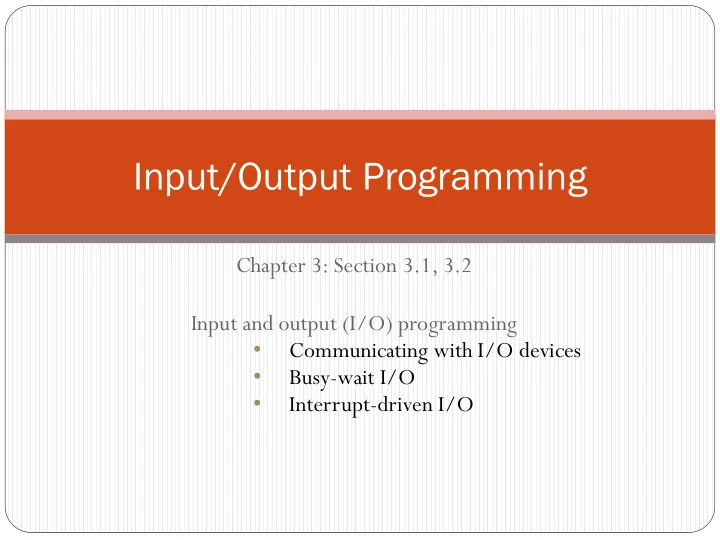
SLIDE 1 Chapter 3: Section 3.1, 3.2 Input and output (I/O) programming
- Communicating with I/O devices
- Busy-wait I/O
- Interrupt-driven I/O
Input/Output Programming
SLIDE 2 I/O devices
CPU status register data register serial port xmit/ rcv control register Baud Rate gen
UART CPU-2-Device Device-2-”Mechanism”
“Devices” may include digital and non-digital components. Example CPU interface - UART device
CPU Bus
- CPU to/from device via register read/write
- I/O “mechanism” effectively transparent to CPU
SLIDE 3 Example: UART for serial communication
Universal asynchronous receiver transmitter (UART) : provides serial
communication – one “character” at a time.
UARTs are integrated into most microcontrollers Allows several communication parameters to be programmed.
Bits/character, Parity even/odd/none, Baud rate, # Stop bits
Example:
time bit 0 bit 1 P no char start stop ... bit n-1
parity bit n data bits
SLIDE 4 UART Registers
Data (read received data, write data to be transmitted) Control register(s) to set:
Bits per character (5,6,7,8 bits). Enable/disable parity generation/checking. Type of parity bit: Even, Odd, Stuck-0, Stuck-1. Length of stop bit (1, 2 bits). Enable interrupt on received byte/end of transmitted byte
Status register(s) to determine:
Receiver Data Ready (Newly-received data in received buffer register) Transmitter Holding Empty (transmit holding register ready to accept new data) Transmitter Empty (All data has been transmitted FE, OE, PE – framing/overrun/parity error in received data
SLIDE 5
Programming I/O
Two types of instructions can support I/O:
special-purpose/isolated I/O instructions; memory-mapped load/store instructions.
Intel x86 provides in, out instructions (“isolated I/O”). Most CPUs (including ARM) use memory-mapped I/O. Special I/O instructions do not preclude memory-mapped I/O.
SLIDE 6 Intel 8051 On-chip address spaces
(Harvard architecture)
Program storage: 0000-0FFF Data address space:
RAM: 00-7F
low 32 bytes in 4 banks of 8 registers R0-R7
Special function registers: 80-FF includes “I/O ports” P0-P3
Special I/O instructions (IN/OUT) for ports P0-P3
Program Memory Data Memory Special Function Registers 0000 0FFF 00 7F 80 FF
SLIDE 7 ARM system memory map (Cortex-M)
Memory-mapped I/O
Program memory addresses
(ROM, Flash)
Data memory addresses (RAM) I/O register addresses
(manufacturer peripherals)
Off-chip (external) memory Off-chip (external) memory Cortex-M peripheral reg’s
(NVIC, SYSTICK, …)
On-chip ROM On-chip RAM External Memory On-chip Peripherals 0x0….0 0x2….0 0x4....0 0x6.…0 0xA….0 0xE.…0
Single address space shared by memory and I/O registers
Cortex CPU peripherals External Devices
SLIDE 8
ARM memory-mapped I/O
Define location(address) for device:
DEV1 EQU 0x40010000
Read/write assembly code:
LDR r1,=DEV1 ; set up device address LDRB r0,[r1] ; read byte from DEV1 MOV r0,#8 ; set up value to write STRB r0,[r1] ; write value to device
Equivalent C code:
Var1 = DEV1; //read from DEV1 to variable DEV1 = Var1; //write variable to DEV1
SLIDE 9
Addressing I/O device registers
Example: STM32Lxx general-purpose I/O port D
; GPIOD module address definitions GPIOD EQU 0x48000C00 ; GPIOD base address MODE EQU 0x00 ; MODE register offset IDR EQU 0x10 ; Input data reg offset ODR EQU 0x14 ; Output data reg offset ; Set up External Memory Controller LDR R0, =GPIOD ;Point to GPIOD regs LDRH R1, [R0, #IDR] ;Read PD15-PD0 pins ORR R1, #1 ;Set bit 0 STRH R1, [R0, #ODR] ;Write to PD15-PD0
SLIDE 10 Addressing I/O registers in C
(from stm32l 32l476x 6xx.h header file)
#define PERIPH_BASE ((uint32_t)0x40000000) /* Peripheral base address in the alias region */ #define AHB2PERIPH_BASE (PERIPH_BASE + 0x08000000) /* AHB1 bus peripherals */ #define GPIOD_BASE (AHB2PERIPH_BASE + 0x0C00) /* GPIO Port D base address */ #define GPIOD ((GPIO_TypeDef *) GPIOD_BASE) /* GPIO Port D pointer */ / * General Purpose I/O */ typedef struct /* Treat GPIO register set as a “record” data structure */ { __IO uint32_t MODER; /* GPIO port mode register, Address offset: 0x00 */ __IO uint32_t OTYPER; /* GPIO port output type register, Address offset: 0x04 */ __IO uint32_t OSPEEDR; /* GPIO port output speed register, Address offset: 0x08 */ __IO uint32_t PUPDR; /* GPIO port pull-up/pull-down register, Address offset: 0x0C */ __IO uint32_t IDR; /* GPIO port input data register, Address offset: 0x10 */ __IO uint32_t ODR; /* GPIO port output data register, Address offset: 0x14 */ __IO uint32_t BSRR; /* GPIO port bit set/reset register, Address offset: 0x18 */ __IO uint32_t LCKR; /* GPIO port configuration lock register, Address offset: 0x1C */ __IO uint32_t AFR[2]; /* GPIO alternate function registers, Address offset: 0x20-0x24 */ } GPIO_TypeDef;
GPIOD->ODR = value; /* write data to ODR of GPIOD */
SLIDE 11 Finding information…
Microcontroller header file defines addresses, record structures,
interrupt numbers, symbolic labels for use in programs.
stm32l476xx.h
Microcontroller reference manual describes manufacturer-designed
modules in the microcontroller (memory, clock, power, peripheral functions and registers, etc.)
Entire “family” of microcontrollers assembled with the same modules STM32L4x5 and STM32L4x6 Reference Manual
Microcontroller data sheet lists details of modules, pins, voltages, etc.
for a specific microcontroller in the family
STM32L476xx Data Sheet
Cortex-M4 Generic User Guide describes ARM-designed functions
Independent of any particular uC manufacturer CPU, Instruction Set, SysTickTimer, NVIC - Nested Vectored Interrupt
Controller, fault detection mechanisms, etc.
SLIDE 12 Busy-wait I/O (“program-controlled”)
Check status Busy? Yes (wait) Access data No (data ready) Check status Busy? Yes (wait) Access data No (device ready)
SLIDE 13 Busy/wait output example
Simplest way to program device.
Instructions test device ready status. OUT_CHAR and OUT_STATUS are device addresses
Normally defined in a “header file” for the microcontroller
/* send a character string */ current_char = mystring; //char string ptr while (*current_char != ‘\0’) { OUT_CHAR = *current_char; //write a character while (OUT_STATUS != 0); //wait while busy current_char++; }
SLIDE 14
Busy/wait output (ARM assy.lang.)
;output character provided in r0 #define OUT_STATUS 0x40000100 #define OUT_CHAR 0x40000104 ldr r1,=OUT_STATUS ;point to status w ldrb r2,[r1] ;read status reg tst r2,#1 ;check ready bit beq w ;repeat until 1 ldr r3,=OUT_CHAR ;point to char strb r0,[r3] ;send char to reg
SLIDE 15
Simultaneous busy/wait input and output
while (TRUE) { /* read */ while (IN_STATUS == 0); //wait until ready achar = IN_DATA; //read data /* write */ OUT_DATA = achar; //write data while (OUT_STATUS != 0); //wait until ready } Above assumes all 8 bits of IN_STATUS are 0 when ready Normally we need to test a single bit: while ((IN_STATUS & 0x01) == 0)
SLIDE 16
Interrupt I/O
Busy/wait is very inefficient. CPU can’t do other work while testing device. Hard to do simultaneous I/O. Interrupts allow device to change the flow of control in
the CPU.
Causes subroutine call to handle device.
SLIDE 17
Interrupt interface
CPU status reg data reg mechanism PC intr request intr ack data/address IR
CPU and device connected by CPU bus. CPU and device “handshake”:
device asserts interrupt request; CPU asserts interrupt acknowledge when it can handle the
interrupt.
SLIDE 18
Interrupt behavior
Based on subroutine call mechanism. Interrupt forces next instruction to be a “subroutine call”
to a predetermined location.
Return address is saved to resume executing
foreground program.
“Context” switched to interrupt service routine
SLIDE 19 Example: interrupt-driven main program
main() { while (TRUE) { if (gotchar) { // set by intr routine OUT_DATA = achar; //write char OUT_STATUS = 1;
//set status
gotchar = FALSE;
//reset flag
} }
} Don’t stop to wait for a character!
Global variables
SLIDE 20 Example: character I/O handlers
#define IN_DATA (*((volatile unsigned byte *) 0xE0028018)) #define IN_STATUS (*((volatile unsigned byte *) 0xE002801C))
void input_handler() { achar = IN_DATA;
//global variable
gotchar = TRUE;
//signal main prog
IN_STATUS = 0;
//reset status
} void output_handler() { } //interrupt signals char done
SLIDE 21 Example: interrupt I/O with buffers
Queue for characters:
head tail head tail a
leave one empty slot to allow full buffer to be detected Queue Array[] Head Tail add_char() remove_char() Queue Class
SLIDE 22
Buffer-based input handler
void input_handler() { char achar; if (full_buffer()) error = 1; else { achar = IN_DATA; //read char add_char(achar); //add to queue } IN_STATUS = 0; //reset status if (nchars >= 1) { //buffer empty? OUT_DATA = remove_char(); OUT_STATUS = 1; } } //above needed to initiate output
SLIDE 23
Interrupts vs. Subroutines
CPU checks interrupt signals between instructions Interrupt handler starting address:
fixed in some microcontrollers usually provided as a pointer (“vector”)
CPU saves its “state”, to be restored by the interrupt handler
when it is finished
Push items on a stack and/or: Save items in special registers
Handler should preserve any other registers that it may use
SLIDE 24
Prioritized interrupts
CPU device 1 device 2 device n D1 D2 .. Dn interrupt acknowledge interrupt requests interrupt controller
Priorities determine what interrupt
gets CPU first.
Vectors determine what code is called
for each type of interrupt.
Mechanisms are orthogonal: most
CPUs provide both.
SLIDE 25
Interrupt prioritization
Masking: interrupt with priority lower than current priority
is not recognized until pending interrupt is complete.
Non-maskable interrupt (NMI): highest-priority, never
masked.
Often used for power-down.
Handler may choose to “enable” other interrupts (allows
handler to be preempted)
CPU may also have bit(s) in its status register to enable or
mask interrupt requests.
SLIDE 26 I/O sequence diagram
:foreground :input :output :queue empty a empty b bc c
receive a send a receive b receive c send b
SLIDE 27 Example: Prioritized I/O
:interrupts :foreground :A :B :C B A,B C A
high priority low priority
SLIDE 28
Interrupt vectors
Allow different devices to be handled by different code. Interrupt vector table:
Directly supported by CPU architecture and/or Supported by a separate interrupt-support device/function
handler 0 handler 1 handler 2 handler 3 Interrupt Vector Table Head
SLIDE 29 Interrupt vector acquisition
:CPU :device receive request receive ack receive vector
Synchronous msg Asynchronous msg
SLIDE 30 Generic interrupt mechanism
intr? N Y
Assume priority selection is handled before this point.
N ignore Y ack vector? Y N timeout? Y bus error call table[vector]
intr priority > current priority?
continue execution
Device sends vector CPU calls handler & Software processes the request CPU acknowledges the request CPU detects interrupt request
N
SLIDE 31
Sources of interrupt overhead
Handler execution time. Interrupt mechanism overhead. Register save/restore. Pipeline-related penalties. Cache-related penalties. Interrupt “latency” = time from activation of interrupt signal
until event serviced.
ARM worst-case latency to respond to interrupt is 27 cycles:
2 cycles to synchronize external request. Up to 20 cycles to complete current instruction. 3 cycles for data abort. 2 cycles to enter interrupt handling state.
SLIDE 32
Exception
Exception: internally detected error.
Example: divide by 0 ARM: undefined opcode, data abort, memory error
Exceptions are synchronous with instructions but unpredictable. Build exception mechanism on top of interrupt mechanism. Exceptions are usually prioritized and vectorized.
SLIDE 33
Trap/Software Interrupt
Trap (software interrupt): an exception generated by an
instruction.
Ex: Enter supervisor mode. Often used to enter operating system (RTOS)
ARM: SWI instruction for traps. Cortex: SVC instruction (supervisor call)