
SLIDE 1
I NTEGRAL Holding www.integral.by Through the element base and - - PowerPoint PPT Presentation
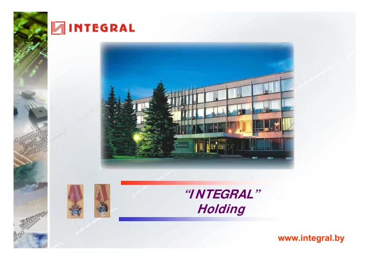
I NTEGRAL Holding www.integral.by Through the element base and display systems to finished microelectronic products Advantages : 50 years of experience in design and production of microelectronic components Complete cycle of
Vitebsk Mogilev Gomel Grodno Pinsk
Molodechno JSC “TSVETOTRON” Diodes, electronics, PCBs
Branch “Transistor” Discrete semiconductor devices, ICs
Brest
Branch “KAMERTON” Silicon wafers, electronics Branch “Semiconductor Device Factory Branch “Belmicrosystems” R&D Center ICs, discrete semiconductor devices, LCD indicators, foundry services, photomasks Branch “ELECTRONICA FACTORY” Electronics JSC “Electromodule” Power semiconductor diodes & rectifier modules
JSC “INTEGRAL” - “INTEGRAL” Holding Managing Company
1961 Starting construction of the main administrative building 1963 Launching Semiconductor Device Factory named after Dzerzhinsky F.E. (Minsk) 1963 Starting construction of “Transistor” factory (Minsk) 1963 First diodes manufactured 1965 First transistors manufactured 1968 “Transistor” factory was put into operation and first transistors were manufactured (Minsk) 1969 Mass production of ICs started 1971 RPC “Integral” amalgamated 1972 Special Design Center of RPC “Integral” launched 1973 First electronic wrist watch “Secunda-2” manufactured 1974 Order of October Revolution is awarded for design and manufacture of instruments for space exploration. 1977 Manufacture of first memory ICs 1978 Manufacture of first microprocessor. 1978 “Electronica Factory” launched (Minsk) 1979 “Kamerton Factory” launched (Pinsk) 1981 The Order of Lenin is awarded for design and manufacture of electronic units for reusable space system ground complex 1982 Manufacture of ALS Logic ICs 1983 “Tzvetotron Factory” launched (Brest) 1986 “Zapad Design Center” launched (Brest) 1988 Manufacture of first lap-tops 1990 Telephone ICs 1991 “Nemiga Design Center” launched (Minsk) 1992 Bank and trade electronic devices 1992 First telephone set made 1993 Calculator ICs
2011 Shipped USD 4.5KK products manufactured at the new submicron production facility 2012 In frames of “BKA” program, manufactured microassemblies and IC assemblies of photosensitive CCD devices for remote sensing satellites 2013 On June 14, 2013, the Ministry of Economy entered “INTEGRAL” Holding into the Public Register of holdings #62 2013 Completion of the design of nonvolatile 1M (128Kx8) FRAM memory 2014 There has been developed and launched into mass production a 16 Mbit CMOS RAM multi-chip module. A set
been developed and put into series production. A mobile artificial lung ventilation apparatus has been developed. 2015 K1643RA014 SRAM IC with the capacity of 1 Mb (128Kx8) manufactured under "silicon on insulator" technology. Software and hardware for identification of reinforced concrete structures. LED lighting system for poultry farms with "sunrise-day-sunset" function. 1994 Logic ICs of HC/HCT, AC/ACT, 4000B series, EEPROM ICs 1995 ICs for one-PCB TV-sets of the 6 generation 1995 Telephone plastic cards 1999 Quality Assurance System is certified for conformance to the requirements of National Standards and International ISO 9001 Standards 2000 Sophisticated VLSI for domestic electronic applications 2001 Development of fast and ultra-fast diodes (FRD and UFRD) 2001 Mastering of special ICs for automotive electronics 2002 Development of ICs for ILA8842 TV processor 2003 Establishment of Integral’s Representative Offices in China and India 2005 MOSFET type power field-effect transistors mass production start up 2005 VLSI development for “BelKa” satellite 2006 0.8 µm ICs mass production start up 2007 Starting production of sophisticated products for medical equipment 2008 Starting production of special purpose 256К memories 2009 0.35 µm IL1307/1356 LSI development 2010 Starting production of special purpose 1 Mbit memories 2010 IC mass production start-up on 200mm wafers 2010 Joint Stock Company “INTEGRAL” established 2011 Start commercial production of 5 products in 0.35μm process node: IN1307, IN1356 – real-time clock ICs, IZ1325 – high-precision RTC IC with thermocompensation, IZ8563 – CMOS timer LSI with 12C-bus RAM, IZ2009 – IC for authentication systems with 1-Wire interface with EEPROM
Pulse Zener Rectifier, medium frequency Varicaps Schottky, power Rectifier-limiter (Zener) Noise generators Noise diodes generators
Pulse diodes Varicaps Power diodes
High-frequency complementary Pulse complementary SHF generator MOS switches
High frequency complementary Pulse complementary Unijunction
Low-voltage, high-frequency, low-noise
Field, N-channel, high voltage
Bipolar, complementary, high-voltage
Complementary, Darlington
Field, high-current, N and P-channel
MOSFET
Semiconductor ICs and Discrete Devices- Manufacturing on the base of Customer's Design (delivery on the base of on-chip testing) Semiconductor and Discrete Devices - Manufacturing on the base of Customer's Design (delivery on the base of wafer PCM testing)
Wafer Fab Service – execution of separate Process Flow Steps or bloks (Metal sputtering, film deposition, EPI-growing, back grinding, wafers testing and so on)
Raw Si substrate manufacturing by Customer's Specs
Process Flows available: Integrated Circuits:
n-MOS CMOS BiCMOS CDMOS BiCDMOS, DMOS Bipolar (TTL, TTL/ALS)
Production Capacities used for Foundry Business:
Production line for 8'' wafers with (0.5-0.35) µm Design Rule Production line for 6'' wafers with (0.8-1.2) µm Design Rule Production line for 4'' wafers with (1.2-3.0) µm Design Rule Basic Process Flows available: Discrete devices: D-MOS ( 1000V) ≤ IGBT-bipolar transistor with isolated gate ( 1500V) ≤ Multi-Epi ( 700V) ≤ Bipolar High-frequency devices ( 300V) ≤ Fabless-business starting from 0.18 µm design rules («Belmicrosystems» Research and Design Center Branch)
0.8µm BiCMOS technology, 3 poly, 2 Ме 0.35µm CMOS technology, 2 poly, 3 Ме High-voltage 0.8µm CMOS technology, 2 poly, 1 Ме Bipolar technologies, 1.5…5 μm, 1-2 Ме 0,8…2 μm BCD, DMOS technologies, 1 Ме Microwave bipolar transistor technology Schottky technology Planar thyristor technology with separation by interdiffuision Epitaxial planar and diffusion planar technologies for manufacturing silicon semiconductor devices , including high-voltage transistors
IC packaging: SO, DIP, P-SOT223-4-1, P-SOT223-4-2, P-TO-5-11, P-TO-5-12, TO-220AB/5, TO-220AB/7, P-TO-220-7-180, P-TO-220-7-230, SIL-3P, SIL-9P, SIL-9MPF, DBS-9P, DBS-9MPF, SOT523-1, SIL-13P, SIL-15P, QFP-80, QFP-100 Semiconductor device assembly:
D2PACK, IPACK, SOT-23,
Household appliances: LCD TV, monitors, microwave ovens, fridges, washing machines. Networking & Telecommunications Telephones, modems, fax machines, electronic dial exchange. Industrial Electronics Automation, instrument engineering, energy flow meters, electric drives, electronic start-control devices. Access Control & Identification RFID-tags, smart key, contactless cards. Space Electronics Satellite-borne electronic equipment,
Payment Systems Plastic bank cards, payment cards, phone cards, prepaid cards for public transport. Agriculture Automated control systems and devices for agriculture and agricultural machinery. Automotive Electronics Fuel injection and ignition systems, turn-indicator systems, wiper systems, lighting equipment.