
SLIDE 1
HYPRES
1
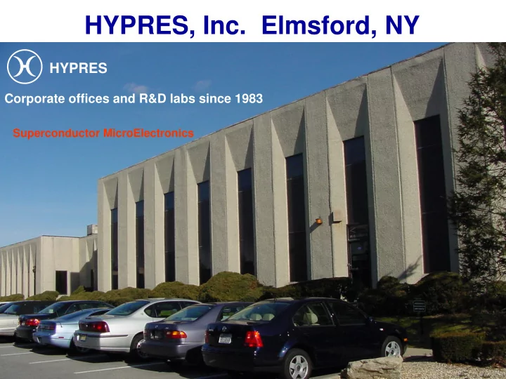
HYPRES, Inc. Elmsford, NY
www.hypres.com
Corporate offices and R&D labs since 1983
HYPRES
Superconductor MicroElectronics
HYPRES, Inc. Elmsford, NY HYPRES Corporate offices and R&D - - PowerPoint PPT Presentation
HYPRES, Inc. Elmsford, NY HYPRES Corporate offices and R&D labs since 1983 Superconductor MicroElectronics HYPRES www.hypres.com 1 HYPRES Technology HYPRES SME technology is HYPRES SME technology is so accurate that it defines the
HYPRES
1
www.hypres.com
Corporate offices and R&D labs since 1983
HYPRES
Superconductor MicroElectronics
HYPRES
2
HYPRES SME technology is HYPRES SME technology is so accurate that it defines the Volt, so accurate that it defines the Volt, so sensitive that it measures brain currents, so sensitive that it measures brain currents, so fast that it directly converts RF signals. so fast that it directly converts RF signals.
Based on a naturally occurring periodic quantum effect Based on a naturally occurring periodic quantum effect — — Rapid Single Flux Quantum (RSFQ) Rapid Single Flux Quantum (RSFQ)
Brings the Power of Digital Processing to the RF Domain Brings the Power of Digital Processing to the RF Domain and changes the Paradigm of Wireless Communications and changes the Paradigm of Wireless Communications
SME = Superconductor Micro-Electronics
HYPRES
3
Unique Features of Superconductor Technology
Speed-of-light transmission in LSI circuits, no RC delay Low-impedance superconductor interconnects have negligible loss, dispersion and crosstalk
Ideal interconnects
SQUID (ADC front-end) is the most sensitive energy detector ~60dB better than conventional semiconductor front end (Example ~ -155dBm for 1 MHz BW, with slope of 20 dBm/decade)
Extremely high sensitivity
Defines the Volt (5ppb accuracy at 10V)
Quantum accuracy
Much less expensive complex chips and facilities/equipment to produce chips than semiconductors (~10 steps, no expensive operations, Thin Film )
Simple, inexpensive IC
fabrication
Receiver System Noise Temperature TS ~ TA (Thermal noise is essentially “0”)
Extremely low noise
Very High-SFDR ADC and DAC (Conversion between analog and digital domains through flux quantum (Φ0 = h/2e) is independent of circuit parameters)
Fundamental linearity using
magnetic flux quantization
10,000X lower than semiconductor technology (Power dissipation for LSIC ~ 1 mW, Switching energy ~ 10-18 J)
Ultra-Low power dissipation
Single Flux Quantum (SFQ) logic is the world’s fastest (Devices ~10X faster than semiconductor, LSI ~ 50X faster than semiconductor)
Ultra-High digital logic speed
Result: Digital-RF Technology
High-fidelity, wideband, high-sensitivity digital representation and subsequent processing (“RF DSP”: channelization/correlation, spectrum control, broadband beamforming,..) of RF waveforms
HYPRES
4
Mobile and Fixed Cellular Satellite Terrestrial Switches and Routers (Military, Commercial, & Civil)
Defense — EW, SIGINT, RADAR, … Ultra-High Speed Computing Instrumentation Medical
HYPRES
5
HYPRES
6
HYPRES Product Benefits for Wireless Networks
Summary
Massively Reduced Network Capital Expenditures
Substantially Reduced Operating Expense Enhanced Revenues and Margins Significantly Enhanced Performance Unparalleled Reliability & Flexibility A “Natural” for Distributed Radio (over fiber, etc.) Boost Spectral Efficiency (HSDPA, etc.) Future-Proof Products -- beyond 3G (>30Mb/s inherent) Extended Mobile Battery Life/Throughput
HYPRES Digital HYPRES Digital-
RF enables the next generation Base Station
HYPRES
7 Analog Filter HPA Digital Signal Processor (MODEM, CODEC, INFOSEC etc.) Digital Down-converter Digital Up-converter Antenna Digital Decimation Filter Digital Interpolation Filter A/D Converter D/A Converter Digital Local Oscillators Dynamic Digital Equalizer Ambient Temperature Electronics Cryogenic Superconductor Electronics
Duplexer
Brings the power of digital processing to the RF domain
HYPRES
8
Complete Digital-RF Transceiver
Total functionality of a base station in a single product
excluding power amplifiers, antenna/tower, and standard ancillary equipment
Commercial Version
Digital-RF Channelizer/ Combiner Network Interface
Network
HYPRES
RF
Baseband DSP Baseband DSP Cryogenic Superconductor Electronics Ambient Temperature Electronics
Enables the All-Digital Software Radio
HYPRES
9
HYPRES Base HYPRES Base Station Electronics Station Electronics
TRx Module Analog To BSC “Lots of” RF Plumbing
Network Interface Network Interface
RF Combiner
PA PA PA PA PA PA
Narrowband Narrowband TRx TRx Narrowband Narrowband TRx TRx DSP DSP DSP DSP Narrowband Narrowband TRx TRx DSP DSP
RF Splitter RF Splitter
Duplexer Duplexer
Software Definable/Programmable No Loss Digital Signal Processing To BSC Broadband Broadband TRx TRx C h a n n e l i z e r C h a n n e l i z e r C
b i n e r C
b i n e r DSPs DSPs
Duplexer Duplexer
H P A H P A Network Interface Network Interface
Traditional Base Traditional Base Station Electronics Station Electronics
vs vs.
. Ultra Wideband for HYPRES SME
GSM
HYPRES
10
Expanded Range of High Maximum Data Rate
Max Min Conventional Receiver HYPRES Receiver
Designed Cell Boundary
Data Rate
HYPRES
11
Conventional Processing Slow, Parallel Hardware HYPRES SME Processing Fast, Serial Hardware Time-sharing of tasks Hardware re-use Uniquely flexible
SCE SCE Receiver Receiver Front Front-
End Digital Digital Correlator Correlator Conventional Conventional Receiver Receiver Front Front-
End Digital Digital Correlator Correlator Digital Digital Correlator Correlator Digital Digital Correlator Correlator SCE SCE Digital Digital Correlator Correlator
HYPRES
12
Multi-User Detection (MUD) for UMTS & CDMA
CDMA systems are severely interference limited Removing interference through multi-user detector can
increase system capacity by 2-10X
This also enables higher data rates, low mobile power, and
easier system administration
Successive Interference Canceller (SIC) is a multi-user
detector scheme for removal of interferers in sequential steps of interference estimation and subtraction
Sequential subtraction provides better interference
cancellation at the expense of greater processing SNR = S/(N+I), N<<I
Tera-Operations DSP Required
HYPRES
13
Partial Partial Crosscorrelation Crosscorrelation Unit Unit Iterative Iterative Linear System Linear System Solver Solver
Antenna
Successive Successive Interference Interference Canceller (SIC) Canceller (SIC)
Why RSFQ?
CMOS cannot do it in real time due to insufficient speed Parallel algorithms are inefficient and often do not converge at all RSFQ SIC is based on a simple Gauss-Seidel iterative algorithm that converges quickly
SME SME Receiver Receiver Front Front-
End SME SME Digital Digital Correlator Correlator
HYPRES
14
Spreading Code Generator & Multiply Accumulate Unit
HYPRES
15
Superior speed of SME can produce independent
multi-Tera-Ops back-end digital signal processor products for conventional transceivers
Successive Interference Canceller (SIC) to sequentially
cancel interferers, starting with the largest one -- Large (up to ~ 10X) increase in capacity
Massively time-multiplexed correlation-based Walsh-
Hadamard (WH) Demodulator -- Large cost savings
Separate WH Demodulators are now used for each multipath of
each reverse link being processed by a base station (parallel processing)
Serialization of tasks using SME processors provide hardware
savings by more than an order of magnitude (serial processing)
HYPRES
16
HYPRES SME Correlation HYPRES SME Correlation-
Based Receivers Provide Optimum Performance in the Digital Optimum Performance in the Digital-
RF Domain
Uses matched waveform to perform digital filtering (correlation) in both the time and frequency domain achieving maximum receive efficiency Hardware is not specific to any analog/digital modulation (FM, PM, MPSK, etc.) or multiple access scheme (FDMA, TDMA, CDMA, MIMO, OFDM, etc.) Real-time Correlator combines functions of downconversion, demodulation, and decoding Direct RF Digital Demodulation in one unit Rapid Φ locking to RF carrier permits tracking of signals with time varying phase and frequency: Tx drift, Doppler-shift, signal hopping, etc. Processes out (suppresses) un-correlated noise & interference over repetitive samples; i.e., increases the system SNR & SIR
Digital Multiplier Digital Correlation Filter/Processor A/D Converter Digital Waveform Generator
Signal characteristics known
In near real time In near real time the optimum matched filter receiver the optimum matched filter receiver
HYPRES
17 Digital Up Converter
Digital-RF Pre-distorter
Digital-to-Analog Converter (DAC) Analog-to-Digital Converter (ADC) HPA Analog BPF Analog BPF Digital LO
Digital Analog
Iin Qin SRF SPD SFB Clock >20 GHz
One HPA Covers Ultra One HPA Covers Ultra-
Wide Bandwidths Consuming Far Less Power
[Multi-Carrier Power Amplifiers]
Near real-time true digital Adaptive Linearization at RF
at RF
Far better than Digital baseband predistorters (Enhanced Efficiency) Feed-forward amplifiers (Lower Distortion) Frequency (& Data Rate) independent from 25% to 50% Clock Rate Efficiency enhancement up to the inherent limit of the HPA Allows use of lower cost HPA
HYPRES
18 Digital Up Converter
Digital-RF Pre-distorter
Digital-to-Analog Converter (DAC) Analog-to-Digital Converter (ADC) HPA Analog BPF Analog BPF Digital LO
Digital Analog
Iin Qin SRF SPD SFB Clock >20 GHz
One HPA Covers Ultra One HPA Covers Ultra-
Wide Bandwidths Consuming Far Less Power
[Multi-Carrier Power Amplifiers] (continued)
Full bandwidth for all air interfaces (waveforms)
passive combining of multiple PAs
Dramatic reduction in overall power consumption*
A/C, power supply, UPS / UPS batteries, cabinet, cooling, and
Allows use of lower cost HPA
Huge reduction in PA and ancillary equipment COST
* Increase of efficiency from 25 to 50% or 75% reduces power dissipation by 66.6% to 90%
HYPRES
19
HYPRES
20
Beam directions defined by setting appropriate
true time delays, corresponding to a wavefront
Set coarse digital delay between antennas by
cross-correlation with discrete steps of 25 ps
Tune digitally controlled analog (continuous)
delays for each antenna by interpolation to <1ps
Beam directions are the same for receive and
transmit due true time delay phasing
Enables multiple beams and adaptive nulling
Significantly augments AJ, LPI, LPD & LPE Further suppression of interference
Note: 1ps is < 1 degree at 2GHz
HYPRES
21 BP ∆-Σ ADC 1 Delay
τ1
BP ∆-Σ ADC n Delay
τn
Correlator (1,n) BP ∆-Σ ADC n+1 Delay
τn+1
BP ∆-Σ ADC 2n Delay
τ2n
Correlator (n+1,2n) BP ∆-Σ ADC N-n+1 Delay
τN-n+1
BP ∆-Σ ADC N Delay
τN
Correlator (N-n+1,N) Pair-Correlator Processor Coarse delay adjustments - Sets coarse beam direction Fine delay adjustments - Refines direction by phase corrections within RF period
HYPRES
22 BP ∆-Σ ADC 1 Delay
τ1j
BP ∆-Σ ADC n Delay
τnj
Delay
τn1−τ11 Digital Accumulator
Adjustments of Delays Digital Cross-correlator
Digital I&Q Filters
Beam j Output BP ∆-Σ ADC 2 Delay
τ2j
BP ∆-Σ ADC i Delay
τij DBF Combiner
Beam-tracking done with Digital-RF
Cross-Correlator
Cross-correlation between antenna-
pairs and delay interpolation
HYPRES
23
Weight Vector 1
τ11w11 τi1wi1 τN1wN1 τ12w1j τijwij τN2wNj τ1Mw1M τiMwiM τNMwNM
Weight Vector j Weight Vector M
Beam 1
Σ Σ Σ
Delay-Multiply Unit
xi xi xi xN xN xN x1 x1 x1
Beam j Beam M
Output of each antenna:
Digitized at RF Split into M digital copies for
M beams
Each copy delayed by TTD (τij) Multiplied by Weights (Wij) Summed to form each of M
beams
k-bit weight Constant, wij 1-bit @40Gbps k×1 Multiplier Delay τij
τijwij
=
Delay-Multiply Unit Delay Control F R O M A D C
( )
ij N i ij j
W t X Y ⋅ − = ∑
=1
τ
The Ultimate in Diversity
HYPRES
24
Omni BS BS1
1
F
u s i n g F
u s i n g N u l l D e p t h N u l l D e p t h Focusing Gain
User User Interferor Interferor Adaptive Adaptive
G N N
Ada ptive Proc e ssing G a in = Ada ptive Proc e ssing G a in = G G + + N N
HYPRES
25
Reduced phase error provides deeper nulls, better C/I :
Phase error using active nulling:
5 degrees of phase error allows deepest null of -27 dB 10 degrees of phase error allows deepest null of -21 dB 20 degrees of phase error allows deepest null of -15 dB
Reduced amplitude error provides deeper nulls, better C/I:
Amplitude error using active nulling:
0.25 dB of amplitude error allows deepest null of -25 dB 0.5 dB of amplitude error allows deepest null of -19 dB 1.0 dB of amplitude error allows deepest null of -13 dB
Digital-RF technology produces ultra-broadband 60 dB nulls: < 0.1 degree in phase < 0.01 dB in amplitude
HYPRES
26 Omni BS BS1
1
F
u s i n g F
u s i n g N u l l D e p t h N u l l D e p t h Focusing Gain
User User Interferor Interferor Adaptive Adaptive
G N N
Ada ptive Proc e ssing Ga in = Ada ptive Proc e ssing G a in = G G + + N N
HYPRES Digital RF technology
It is better to increase N (nulling) than increase G (antenna gain)
Increasing G requires larger antennas
Increasing N requires finer and more stable amplitude and phase
HYPRES
27
Makes virtually any antenna set into adaptive arrays
Significantly improves the C/I by (very) many dBs
combined with these other alternatives for added improvements
Spatial Diversity – –minimizes fading and effects of multipath propagation, and reduc minimizes fading and effects of multipath propagation, and reduces es the effective delay spread of the channel, allowing higher bit r the effective delay spread of the channel, allowing higher bit rates to be supported. ates to be supported.
Balances the forward and reverse links + Adaptive Sub-Sectorization -- ultimate in performance
Enables HUGE increases in Range/Capacity/Flexibility for GSM, CDMA, GPRS, EDGE, UMTS, and beyond
HYPRES
28
Multiple Input/Multiple Output (MIMO) requires very accurate time synchronization, and ability to discriminate/extract signals on the same frequency with the same code.
Digital Digital-
RF Correlator:
time and frequency domain achieving maximum receive efficiency
phase and frequency
Correlates UMTS user signals in same band and same code separated by only 6 inches
HYPRES
29
(continued)
Correlates UMTS user signals in same band and same code separated by only 6 inches
Digital Digital-
RF offers an unprecedented and exceptionally cost-
effective solution that has the potential to increase capacity on forward and rever that has the potential to increase capacity on forward and reverse links by 10 X se links by 10 X
HYPRES
30
50 100 150 200 250 300 350 400 450 500 0% 20% 40% 60% 80% 100% 120%
Base Station Cell Area Data Rate (kbps)
Digital-RF Conventional
One Digital-RF Base Station
[versus 10 to 14 Conventional] Example: EDGE (MCS-9) = 470 kbps
HYPRES
31
Peak Data R ate Peak Data R ate 70 kbps (MCS 1) 140 kbps (MCS 4) 240 kbps (MCS 6) 470 kbps (MCS 9) Conventional Conventional HYPR E S Digital HYPR E S Digital-
F R F
Unparalleled Performance – Dynamically* Allocated Resources
[* measured in nanoseconds]
Can dynamically adjust to traffic density, including “inverse breathing”
HYPRES
32
Day Night
High Low Med-High Med-Low
Traffic Density
Unparalleled Performance – Dynamically* Allocated Resources
[* measured in nanoseconds]
HYPRES
33
Peak Data R ate Peak Data R ate 70 kbps (MCS 1) 140 kbps (MCS 4) 240 kbps (MCS 6) 470 kbps (MCS 9) Conventional Conventional HYPR E S Digital HYPR E S Digital-
F R F
an option to geo-locate using multiple towers w/o use of location devices in mobiles
and cross link to central sites
(prior to processing) is a natural for fiber or microwave connection
HYPRES
34
HYPRES Digital-RF Infrastructure
Fundamental Proof of Performance Established
Multi-chip Module Packages (MCM) Digital-to-Analog Converter (DAC) Multiplier Low-jitter On-chip Clock Correlator Digital I&Q Converters Analog-to-Digital Converter (ADC) Optical I/O and Packaging User Interfaces Shift Register Random Access Memory (RAM) Delay line
HYPRES
35
Low-temperature Superconductor (Nb) ICs
Time-to-digital Converter with on-chip 40 GHz clock 15-bit Analog-to-digital Converter with 20 GHz clock (98dB SFDR@ 10 MHz) 1cm x 2 cm 10 Volt Chip with 5ppb accuracy (>20,000 Josephson junctions) Transient Digitizer: Two 6- bit 20 GSa/s Flash ADCs with 32-word memory Two-channel Dual-function Digitizer (TDC & ADC) Multi-chip Module (20 Gbps interchip data rate) Two-channel Digital Channelizer (>12,000 JJs)
HYPRES
36
Benchmark Performance Metric for Digital Logic
100 200 300 400 500 600 700 800 1980 1985 1990 1995 2000 2005
Year Digital Divider Frequency (GHz) III-V HBT Si BJT SiGe HBT FET/HEMT CMOS SME
3 µm 1.75 µm 1.25 µm 0.25 µm
Logic Speed: Superconductor vs. Semiconductor
~ 10 X Faster ~ 10 X Faster
0.8 µm
HYPRES
37
Operational Region at Different Input Frequencies (set of output voltages vs. current supply)
40 80 120 Input Frequency GHz
Input Output Current bias
Current Bias
HYPRES
38
220 GHz Operation of a Toggle Flip-flop (1.75-µm)
HYPRES’ 1.75-µm, 5 kA/cm2, CMP Nb Josephson fabrication process
11 JJs (9 JJ RSFQ T flip-flop + 2 JJ I/O)
Fin Fout
Fin Input Frequency [GHz]
Fout =
Fin/out = V·(1/Φ0) = V·KJ where, KJ = 483.597898(19) x 106 Hz/µV
220 GHz
Fout Output Frequency [GHz] 0.1 0.2 0.3 0.4 50 100 150 200 50 100 25 75 Input Voltage [mV]
Fin 2
0.5 0.0 250 125
HYPRES
39
240 GHz Operation of a Toggle Flip-flop (1.5-µm)
Operational Region at Different Input Frequencies (set of voltage differences vs. current)
Input Output Current bias Input Frequency
1 2 3 4 5 6 7 8 50 100 0.05 0.1 0.15
240 GHz
ε
Current Bias SUNY’ 1.5-µm, 6 kA/cm2, CMP Nb Josephson fabrication process
HYPRES
40
395 GHz Operation of a Toggle Flip-flop (0.8-µm)
Operational Region at Different Input Frequencies (set of voltage differences vs. current)
Difference (Fin - 2 * Fout ) 0.005 mV/div Increasing Input Frequencies
0.0 0.2 0.4 0.6
395 GHz
Margin Bias (mA)
Input voltage sense Output Margin bias Input current SUNY’ 0.8-µm, 20 kA/cm2, CMP Nb Josephson fabrication process
HYPRES
41
0.25-µm Nb Fabrication Process DFD operation for ƒOUT = ½ ƒIN
Upper Bound on Error Rate
0.1
Voltage (mV)
0.75 1.25 1.50 1.00 0.50
V = Φ0 · fJ [bits / second] - or - fJ = V·(1/Φ0) = V·KJ where, KJ = 483.597898(19) x 106 Hz/µV [accuracy 0.39 ppb]
CERTI FI ED
Fundamental Physical Constant
SUNY’ 0.25-µm, 140 kA/cm2, CMP Nb Josephson fabrication process
HYPRES
42
A 1 GHz Band-Pass ADC Test Chip
2nd order Digital Filter
Digital Downconverter Clock in
1st order Digital Filter
Signal in 1 GHz 1 GHz Sigma-Delta band-pass 1st-order modulator
3 micron process,
20 GHz clock
Two digital filters:
1st order 8-bit filter 2nd order 15-bit filter
High-Speed Functionality has been successfully proven: 1 GHz signal has been directly digitized and digitally downconverted to baseband
HYPRES
43
A 5 GHz Band-Pass ADC Test Chip
5 GHz Sigma-Delta band-pass 2nd-
2nd order Digital Filter
Digital Downconverter Clock in 18 GHz
1st order Digital Filter
Signal in 5 GHz
3 micron process,
20 GHz clock
Two digital filters:
1st order 8-bit filter 2nd order 15-bit filter
High-Speed Functionality has been successfully proven: 5 GHz signal has been directly digitized and digitally downconverted to baseband
HYPRES
44
3 cm
HYPRES LTS (Nb) MCM
Channelizer #1
ADC
Channelizer #2
HYPRES
45
HYPRES
46
Performance/Reliability far exceeding conventional electronics
Wireless cellular communications (HTS filters) Mine detection Highest sensitivity radar receivers IR imaging systems
Reliability (demonstrated MTBF of 90+ years) Ruggedness (proven in space environment) Combat environment (proven in IR imaging systems) Efficiency (MEMS package)
choices and selection:
Commercial vendors (Leybold, Air Liquide, Sumitomo) Military contractors (Ball Aerospace, Lockheed Martin) Small Business (TAI, Sunpower, Creare)
HYPRES
47
Cryocooled superconducting filters fielded today in military systems
Conforms to all military specifications
Cryocooled superconducting filters fielded today in commercial cellular base stations
99.999% Uptime, MTBF of 90+ years
Cryocoolers deployed in space
Passed space qualification
Cryocoolers used in vacuum systems in semiconductor foundry
Conforms to highest reliability requirements
HYPRES
48
HYPRES
49
HTS leads provide excellent
electrical conductance and reduced thermal conductance
Output multiplexing reduces
number of output leads
Bias current recycling reduces
number of DC Bias lines
Radiation load can be reduced
by use of intermediate temperature shields
50 100 150
Size, Weight, And Power (SWAP) vs. Heat Load
SWAP Heat Load (mW)
HYPRES
50
Minimize size, weight and power of the cryocooler
Past 2 kW Near Term < 1.5 kW 19” x 5 ft 19” x 2 ft
Multi-channel Commercial Tx/Rx
Present ~ 1.3 kW 19” x 16”
10-channel Military Tx/Rx
250 – 500 cu.in. 150 – 300 W
HYPRES
51
Power Supply Cryocooler with Packaged SME MCM Controller Interface Electronics
6” x 8” x 10” = 480 in3 [for 10 channels]
4 to 10 Channel Transceiver SME MCM Power Amplifier Interface Module
HYPRES
52
[JTRS]
ADC 1 ADC 2 ADC m m×n Digital Switch Matrix Digital I&Q Down Converter Digital I&Q Decimation Filter Digital Channelizer Unit 1 Digital I&Q Down Converter Digital I&Q Decimation Filter Digital Channelizer Unit n Baseband Digital Signal Processor (Receive) [Further Channelization, Demodulation, Decoding, Despreading,…] Predistorter /DAC 1 n×m Digital Switch Matrix Digital I&Q Up Converter Digital I&Q Interpolation Filter Digital Transmitter Unit 1 Digital I&Q Up Converter Digital Transmitter Unit n Baseband Digital Signal Processor (Transmit) Digital I&Q Interpolation Filter Predistorter /DAC 2 Predistorter /DAC m PA 1 PA 2 PA m Note: For a (JTRS) 10-channel 2-2000 MHz transceiver, n = 10, m = 3 to 5 Receiver Transmitter SME RTE
HYPRES
53
% of Current Price Number of Carriers/Sector – 3 Sectors
0% 10% 20% 30% 40% 50% 60% 70% 80% 1 2 3 4 5 6 7
% of Current Price
HYPRES
54
0% 10% 20% 30% 40% 50% 60% 70% 1 2 3 4 5 6
% of Current Price Number of Carrier/Sector – 3 Sectors
% of Current Price
HYPRES
55
[and TD-SCDMA]
% of Current Price Number of Carriers/Sectors – 3 Sectors
0% 10% 20% 30% 40% 50% 60% 70% 1 2 3 4 5 6 7 % of Current Price
HYPRES
56
HYPRES Product Benefits for Wireless Networks
Summary
Massively Reduced Network Capital Expenditures
Substantially Reduced Operating Expense Enhanced Revenues and Margins Significantly Enhanced Performance Unparalleled Reliability & Flexibility A “Natural” for Distributed Radio (over fiber, etc.) Boost Spectral Efficiency (HSDPA, etc.) Future-Proof Products -- beyond 3G (>30Mb/s inherent) Extended Mobile Battery Life/Throughput
HYPRES Digital HYPRES Digital-
RF enables the next generation Base Station
HYPRES
57
Brings the Power of Digital Processing to the RF Domain Brings the Power of Digital Processing to the RF Domain and changes the Paradigm of Wireless Communications and changes the Paradigm of Wireless Communications
HYPRES
58
HYPRES
59
Wideband A/D Modulator
∆f1 ∆fi ∆fn
f1+∆f1 f1 fi+∆fi fi fn+∆fn fn
f1
Digital Channelizer
Analog Input Digital Mixer Digital Filter Digital Mixer Digital Filter Digital Mixer Digital Filter fi fn ∆f1 ∆fi ∆fn
Programmable Band-location and Bandwidth Selection
Simultaneous reception of multiple narrowband signals with single wideband ADC Sub-bands digitally extracted with programmable band location and BW
HYPRES
60
Wideband A/D Modulator
Programmable Digital LPF
Digital LO 90°
Controller Define ∆fi Define fi Define ∆fi
Digital Baseband Output
Programmable Digital LPF
I Q Analog RF Input
1-bit oversampled 20-40 Gbps digital code 1-bit Multiplier 1-bit Square wave
“1 1 1 1 0 0 0 0” “1 1 0 0 0 0 1 1”
High Dynamic Range (SFDR)
HYPRES
61
4 GHz bandwidth /16
GHz clock
16 correlator channels 9-bit output values 1600 devices 5 mm x 5 mm chip
size
DSP blocks include Multipliers Accumulators Adders
[Result of a Phase I STTR]
HYPRES
62
Integration Time [sec]
10
10
10
10
10
10
10 10
1
10
2
Signal to Noise Ratio Improvement [dB]
1-bit HYPRES Demonstrated (4 GHz BW) 2-bit HYPRES Goal (10 GHz BW)
HYPRES
63
DC/SFQ 16-stage Shift Register 16-stage Shift Register 16 x 9 Accumulator Bank
Clock Signal
Bitwise-XOR
... ...
DC/SFQ SFQ/DC SFQ/DC
Signal Monitor Clock Monitor
SFQ/DC SFQ/DC SFQ/DC
5 mm
Test sequence when a train of 2X16+2=34 ‘1’s
(signal “DATA”) is loaded into the circular shift register.
The correct operation of all 16 XOR gates for all
possible combinations of inputs (“00”, “10”, “01”, “11”) and correct operation of circular shift register under full load.
16-Lag “it works”
HYPRES
64
5 mm
Data output after 16 cycle delay with S0=S3=S5=1 and S1=S2=S4=0 Clock output Data input monitor Clock input monitor Data input Clock input Data output after 16 cycle delay with S0=S3=S5=1 and S1=S2=S4=0 Clock output Data input monitor Clock input monitor Data input Clock input
~ 1500 JJs
“it works”
HYPRES
65 2 4 6 8 10 12 14 16 18 20 1.E+06 1.E+07 1.E+08 1.E+09 1.E+10
Nyquist Sample Rate (Sample/s) Effective Number of Bits (ENOB)
40 GHz, 1st order, 2-level quantizer 40 GHz, 2nd order, 5-level quantizer 160 GHz, 2nd order, 2-level quantizer 160 GHz, 1st order, 2-level quantizer
106 107 108 109 1010
Nyquist Sample Rate (Samples/s)
HYPRES demonstrated 13 GHz ADC HYPRES demonstrated 13 GHz ADC
HYPRES
66
At 5 K, thermal noise is 60x less
than at room temperature
ADC only produces a
“quantization error” (IN)
With dither, IN has a noise-like
spectrum
Noise Temperature (TN)
L2 = Front-end inductance m = # of synchronizer channels fclk = Clock frequency ∆f = signal bandwidth
clk clk B s B N N
f f f f km L k f k R I T ∆ ∝ ∆ ⎟ ⎠ ⎞ ⎜ ⎝ ⎛ Φ = =
2 2 2
12 ) ( π
0.001 0.01 0.1 1 10 0.1 1 10 100
Bandwidth (MHz) Noise Temperature (K)
3 um, fclk=12.8 GHz 1.5 um, fclk=40 GHz 0.8 um, fclk=80 GHz 0.4 um, fclk=160 GHz
ADC does not degrade the system noise temperature
HYPRES
67
Sensitivity (∆I) is the least
significant bit (LSB)
M = Mutual inductance m = Number of synchronizer
channels
fclk = Clock frequency ∆f = signal bandwidth N = Oversampling ratio = fclk/(2fs) clk
f f N Mm I ∆ ∝ Φ = ∆ 2
0.1 1 10 100
Bandwidth (MHz) Sensitivity (dBm)
3 um, fclk=12.8 GHz 1.5 um, fclk=40 GHz 0.8 um, fclk=80 GHz 0.4 um, fclk=160 GHz
clk
f f R I
2 2
∆ ∝ ∆
Slope = 20 dBm/decade
R = 50 Ω
SQUID, used as ADC front-ends, is the most sensitive energy detector
~ 60dB better than conventional
HYPRES
68
Deep FFT Measurements Show >100 dB SFDR
Decimation to Nyquist band
HYPRES
69
10 20 30 40 50 60 70 < 2 GHz 2-6 GHz 6-10 GHz 10-20 GHz 20-45 GHz 45-55 GHz 1st Generation (20-25 GHz) 3rd Generation (80-100 GHz) 4th Generation (160-200 GHz) 2nd Generation (40-50 GHz) Direct Digital-RF One Stage
Mixing To ~5 GHz IF Direct Digital-RF One Stage
Mixing To ~5-10 GHz IF Direct Digital-RF One Stage
Mixing To ~5-20 GHz IF Direct Digital-RF One Stage of Mixing Clock Frequency
Digital-RF: Digitization and Digital Processing at multi-GHz RF
G r
t h
N b L a r g e
c a l e D i g i t a l I C T e c h n
y
2003-2004
HYPRES
70
HYPRES
71
HYPRES SME technology is HYPRES SME technology is so accurate that it defines the Volt, so accurate that it defines the Volt, so sensitive that it measures brain currents, so sensitive that it measures brain currents, so fast that it directly converts RF signals. so fast that it directly converts RF signals.
Based on a naturally occurring periodic quantum effect Based on a naturally occurring periodic quantum effect — — Rapid Single Flux Quantum (RSFQ) Rapid Single Flux Quantum (RSFQ)
Brings the Power of Digital Processing to the RF Domain Brings the Power of Digital Processing to the RF Domain and changes the Paradigm of Wireless Communications and changes the Paradigm of Wireless Communications
SME = Superconductor Micro-Electronics
HYPRES
72
Commercial Primary Voltage Standard for Metrology
1cm x 2 cm 10 Volt Chip with 5ppb accuracy (23,000 Josephson junctions) Cryocooled Voltage Standard System This application cannot be done using any other technology...
HYPRES
73
Fetal Magneto-Cardiogram (fetal heart currents detection) Magneto-Encephalogram (brain currents detection)
Hypres/BTi FMCG System CTF MEG System
Examples of Commercial SQUID-based Magnetometers
(SQUID - Superconducting QUantum Interference Device)
These applications cannot be done using any other technology...
HYPRES
74
Zero Resistance Expulsion and Quantization of Magnetic Flux
Φ = ∫BndA = n Φ0 Φ0 = h/2e = 2.07 mV•ps
= 2.07 x10⁻¹⁵ Wb
Single Flux Quantum (SFQ)
B
T < Tc I V I V
T > Tc T < Tc
HYPRES
75
Superconductor Thin Insulator Superconductor
Ic
Φ0
Ib Ib Ib
Ic Ic
Φ0
Ib
Ic Ic
I= Ic sin(φ) I
Memory cell Josephson Junction
Typical Critical Current: Ic ~ 0.1 mA Time constant : τ ~ 1 ps (3-µm process) τ ~ 0.1 ps (0.2-µm process)
Φ0
I < Ic
JJ stays superconductive
I > Ic
JJ goes resistive and passes magnetic flux through
Active component (switch) in superconductor electronics
HYPRES
76
Microstrip Lines can ballistically transfer picosecond waveforms
Generator Receiver Matched microstrip line
Semiconductor VLSI speed is limited by interconnect delays (RC- type charging) Superconductors have unique capability to transfer picosecond waveforms without distortions with speed approaching speed of light Crosstalk between neighboring transmission lines is very small Josephson junction impedance can be matched to that of microstrip lines
HYPRES
77
Picosecond waveforms and time responses
I V
Ic
I V
Ic
RSFQ Logic
“1” “0”
∫ Vdt = Φ0
SFQ pulses with quantized areas
(picosecond front and tail)
Voltage pulses
(picosecond front, nanosecond tail)
Latching logic
70-80’s 90’s
Adding a shunt resistor allows the generation of separate SFQ pulses
HYPRES
78
Non-storage Inductance (~6 pH) Junction Shunt (~1 Ω) Junctions of different area (min. area = 3 µm x 3 µm) Storage Inductance (~12 pH)
Toggle Flip-Flop Layout
HYPRES
79
Synchronous pulse coding
Logic “1” - presence of a data SFQ pulse between two clock SFQ pulses Logic “0” - absence of a data SFQ pulse between two clock SFQ pulses
SFQ pulses
∫Vdt = Φ0 = h/2e = 2.07 mV·ps
Both Data and Clock are SFQ voltage pulses V(t) with quantized areas
RSFQ - Rapid Single Flux Quantum
HYPRES
80
How to generate, transfer, store, and switch SFQ pulses
Non-storage inductance ~ 6 pH vs. Storage inductance ~ 12 pH
HYPRES
81
Synchronous pulse coding
SFQ pulses
∫Vdt = Φ0 = h/2e = 2.07 mV·ps
Both Data and Clock are SFQ voltage pulses V(t) with quantized areas
Φ0
Josephson Junction
Typical Critical Current: Ic ~ 0.1 mA Time constant : τ ~ 1 ps (3-µm process) τ ~ 0.1 ps (0.2-µm process)
IC
HYPRES
82
Data Presentation Natural quantization Power consumption Power supply Self-timing possible Maximum IC Speed Latching logic Voltage No ~ 3 pW/gate AC No ~ 3 GHz RSFQ logic Magnetic flux Yes (Φ0 = h/2e) ~ 0.3 pW/gate DC Yes ~ 300 GHz
HYPRES
83
Non-storage Inductance (~6 pH) Josephson Junctions with different Ic Storage Inductance (~12 pH) J1 J2 J4 J3 L Ib Clock/Reset Out Set
internal memory gate-level pipelining high-throughput circuits ultra-low power dc bias only local timing
HYPRES
84
Basic Set of RSFQ Elementary Cells
T flip-flops, RS flip-flops, and their modifications with DRO/NDRO
FF
NR
FF
DR
FF
CSSA
FF
Σ
2.6 m V 2.6 m V 2.6 m V 2.6 m V
D flip-flop D flip-flop with AND Carry-Save Serial Adder
HYPRES
85
Phase (Time Delay) Modulation-Demodulation Architecture
Accurate measurement of time delays modulated by input signal
Modulation: Clock generates two identical SFQ
pulse trains (D goes via Quantizer, T goes via a delay)
Input signal induces additional
current in the Quantizer
This additional current changes
time of releasing SFQs of train D from the quantizer
Demodulation: T and D SFQ pulse trains meet at
the synchronizer (race arbiter)
change in arrival time of train D vs.
train T is measured in synchronizer
D D T T
HYPRES
86
Performance Metric: Power-Delay Product
1 10 100 1000 1.E-04 1.E-03 1.E-02 1.E-01 1.E+00 1.E+01 1.E+02 1.E+03
Power Dissipation per Gate Time Delay per Gate (ps) 100 aJ 1 a J 2 aJ 1 fJ 10 fJ 100 fJ 1 pJ 10 pJ
0.1 µW 1 µW 10 µW 100 µW 1 mW 10 mW 100 mW 1 W
100 pJ
InP HBT
1 aJ
>4 Orders-of-Magnitude
Si CMOS SOI CMOS AlInAs HBT SiGe HBT Si BJT Si BJT RSFQ(Nb) Semiconductor Trend Projection
>6 Orders-of-Magnitude
HYPRES
87
MAG Metal Deposition System 1988 6" Coat & Develop Track 2001 0.8-µm Projection Aligner 2001 High-Jc Trilayer Deposition 1997 6" Wafer Dicer 1998 1999 Chem.-Mech. Polisher PECVD Oxide Deposition 2003 Oxide Etching System 2003 Metal Etching System 2003 E-beam Metal Deposition 2003 1.0-µm Contact Aligner 2003 Flip-Chip MCM Bonder 2004
4 Nb (superconductor) metal layers 2 resistor layers 1 Nb-AlO-Nb Josephson junction trilayer
R 3 M 3 M 2 M 1 R 2 M 0 S i O 2
Major Fabrication Facility Upgrade in 2003-2004
HYPRES
88
Founded in 1983, HYPRES is a complete superconductor
electronics company, offering design development, fabrication, testing, and packaging in a commercial production environment
Privately-held Small Business in Elmsford, NY, located 30 miles
north of New York City
Team of 40 (mostly advanced degreed) 16,000 sq. ft. facility includes commercial Nb foundry
HYPRES is the premier commercial supplier of Primary
Voltage Standard circuits and systems worldwide
HYPRES commercial Nb Foundry has 8-10 mask releases
per year and offers individual chip sites at only $80/mm2
For more information visit http://www.hypres.com