
SLIDE 1
Yale West Campus Materials Characterization Core (MCC) ywcmatsci.yale.edu
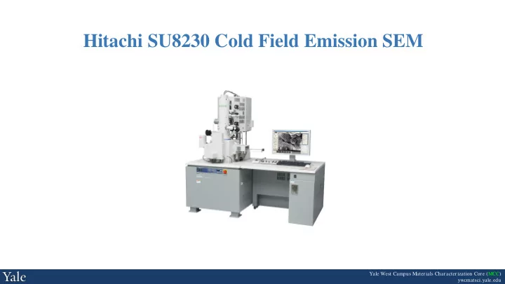
Hitachi SU8230 Cold Field Emission SEM Yale West Campus Materials - - PowerPoint PPT Presentation
Hitachi SU8230 Cold Field Emission SEM Yale West Campus Materials Characterization Core (MCC) ywcmatsci.yale.edu Core Policies DO NOT let other people use the facility under your account. DO NOT try to fix parts or software issues by
Yale West Campus Materials Characterization Core (MCC) ywcmatsci.yale.edu
Materials Characterization Core (MCC) ywcmatsci.yale.edu
2/20
Materials Characterization Core (MCC) ywcmatsci.yale.edu
3/20
Electron source Condensor lens 1 Condensor lens 2 Objective lens Sample Objective aperture Deflection coils
Materials Characterization Core (MCC) ywcmatsci.yale.edu
4/20
Brightness: 105 A/cm2sr Beam size = 50 - 100 kÅ Operation temperature: 3000 K Vacuum: 10-5 Torr Lifetime: 300 hrs
Brightness: 10 x Beam size = 50- 100 kÅ Operation temperature: 2500 K Vacuum: 10-7 Torr Lifetime: 500 - 1000 hrs
Brightness: 500 x Beam size = 100 - 250 Å Operation temperature: 2500 K Vacuum: 10-9 Torr Lifetime: > 4000 hrs Brightness: 1000 x Beam size = 30 - 50 Å Operation temperature: 300 K Vacuum: 10-11 Torr Lifetime: > 10000 hrs
Acc Voltage Extraction Voltage
Materials Characterization Core (MCC) ywcmatsci.yale.edu
5/20
p2: Object distance of objective lens q2: Image distance of objective lens WD: Working Distance between the bottom of the
dG: Beam size exiting the gun p1: Object distance of condenser lens q1: Image distance of condenser lens
Materials Characterization Core (MCC) ywcmatsci.yale.edu
6/20
Penetration depth
SEM images of vanadium oxide nanotubes at different acc voltages
Image courtesy http://www.microscopy.ethz.ch/
Materials Characterization Core (MCC) ywcmatsci.yale.edu
7/20
200 um aperture and 10 mm WD. 200 um aperture and 38 mm WD
Materials Characterization Core (MCC) ywcmatsci.yale.edu
8/20
Sample Electron beam CL X-ray (1-3 µm) Continuous X-ray EDX (1-3 µm) BSE (~300 nm) SE (5–50 nm) AE (1-5 nm)
Topographical information
Composition (atomic number) and topographical information
information (Energy Dispersive X-ray Spectroscopy)
information
charging
Materials Characterization Core (MCC) ywcmatsci.yale.edu
9/20
Goldstein et al. 1981
50 eV 2000 eV
SE AE BSE Elastic reflection
Materials Characterization Core (MCC) ywcmatsci.yale.edu
10/20
can not be machined to perfect symmetry.
beam: a disk of minimum confusion
narrower beam diameter
wider diameter
stigmator coils circular beam
Materials Characterization Core (MCC) ywcmatsci.yale.edu
11/20
E-beam (0.5–30 kV) Sample Faraday Cage
Optical waveguide Electron Multiplier Dynodes 1-2 kV Output Photocathode SE<50 eV Scintillator +10kV BSE
electrons are attracted by +200 V on grid and accelerated onto scintillator by +10 kV bias;
scintillator (phosphor surface) passes along light pipe to external photomultiplier (PM) which converts light to electric signal.
detected but less efficiently because they have higher energy and are not significantly deflected by grid potential.
Materials Characterization Core (MCC) ywcmatsci.yale.edu
12/20
Materials Characterization Core (MCC) ywcmatsci.yale.edu
13/20
SE + BSE signal
Sample courtesy of : Nagaoka University of Technology, Faculty
Materials Characterization Core (MCC) ywcmatsci.yale.edu
14/20
Sample courtesy of : Nagaoka University of Technology, Faculty
Materials Characterization Core (MCC) ywcmatsci.yale.edu
15/20
Sample courtesy of : Nagaoka University of Technology, Faculty
Materials Characterization Core (MCC) ywcmatsci.yale.edu
16/20
electrode
Materials Characterization Core (MCC) ywcmatsci.yale.edu
17/20
specimen, thereby slowing down the primary electron beam to the desired landing energy.
Vlnd = Vacc – Vrtd; Vrtd : Deceleration voltage
Vacc: 500 V Magnification: 100kx
Al electrolytic capacitor
Vacc: 500 V Magnification: 100kx
Courtesy of St. Jude Medical, CRMD-U.S.A.
y electron
Materials Characterization Core (MCC) ywcmatsci.yale.edu
18/20
information can be obtained simultaneously with the secondary electron image.
differentiation on materials of similar density.
Specimen: Carbon nanotubes Vacc: 30 kV Magnification : 250kx BF-STEM image Internal information DF-STEM image surface information
SE detector Photon guide
STEM detector
Materials Characterization Core (MCC) ywcmatsci.yale.edu
19/20
SnTe nano-plate Au contact SiO 2 substrate I+ I- V+ V- V+ V-
Materials Characterization Core (MCC) ywcmatsci.yale.edu
20/20