
SLIDE 1
Digital Systems
Calcolatori Elettronici e Sistemi Operativi
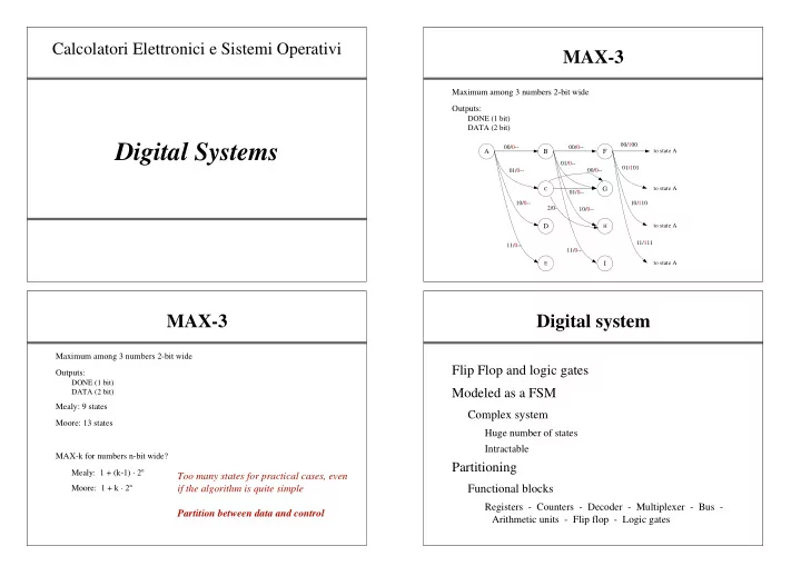
MAX-3
A B
C
D
E
00/0-- 01/0-- 10/0-- 11/0--
F G
H
I
00/0-- 01/0-- 10/0-- 11/0-- 00/100 01/101 10/110 11/111 to state A to state A to state A to state A 00/0-- 01/0-- 2/0-
Maximum among 3 numbers 2-bit wide Outputs:
DONE (1 bit) DATA (2 bit)
MAX-3
Too many states for practical cases, even if the algorithm is quite simple Partition between data and control
Maximum among 3 numbers 2-bit wide Outputs:
DONE (1 bit) DATA (2 bit)
Mealy: 9 states Moore: 13 states MAX-k for numbers n-bit wide? Mealy: 1 + (k-1) · 2n Moore: 1 + k · 2n
Digital system
Flip Flop and logic gates Modeled as a FSM
Complex system
Huge number of states Intractable
Partitioning
Functional blocks
Registers - Counters - Decoder - Multiplexer - Bus - Arithmetic units - Flip flop - Logic gates