
SLIDE 1
1
Advanced Digital IC-Design
Designing for Low Power
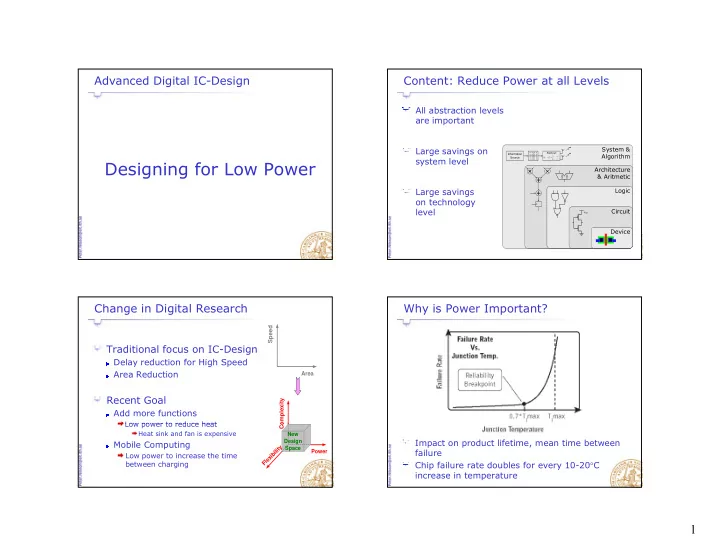
All abstraction levels are important
Content: Reduce Power at all Levels
Large savings on system level Large savings
System & Algorithm Architecture & Aritmetic Logic
ADD SUBInformation Source
[ ] * 1 2 1 2 * 2 1 c c u u c c ⎡ ⎤ − → ⎢ ⎥ ⎣ ⎦ Alamoutig g
- n technology
level
VDDDevice Circuit
Change in Digital Research
Traditional focus on IC-Design
D l d ti f Hi h S d
Speed
Delay reduction for High Speed Area Reduction
Recent Goal
Add more functions
Low power to reduce heat
- mplexity
Area
Low power to reduce heat
Heat sink and fan is expensive
Mobile Computing
Low power to increase the time between charging
Co Power F l e x i b i l i t y New Design Space
Why is Power Important?
Impact on product lifetime, mean time between failure Chip failure rate doubles for every 10-20°C increase in temperature