delivery expected in october 2015
play

Delivery expected in October 2015. The delivery of power amplifiers - PowerPoint PPT Presentation

PSB RF bypasses + PSB TFB electronics Executive summary: Components for the PSB rf-bypasses will be installed (Joao BENTO) on the 15 th of June 2015 in the PS to be tested with beam currents equivalent to those expected in the PSB with Linac 4.


  1. PSB RF bypasses + PSB TFB electronics Executive summary: Components for the PSB rf-bypasses will be installed (Joao BENTO) on the 15 th of June 2015 in the PS to be tested with beam currents equivalent to those expected in the PSB with Linac 4. The new electronic circuits for the PSB TFB have been produced and their firmware is starting the testing phase. Delivery expected in October 2015. The delivery of power amplifiers (800 W instead of 100 W) foreseen for mid 2016 is a source of worry. A rf management meeting should be held soon to address this issue. A. Blas PSB-LIU meeting 04 Jun 2015 1

  2. PSB RF bypasses Presently installed hardware 3 times 0.5 Ω /1 W in series with 4 x // 100nF A. Blas PSB-LIU meeting 04 Jun 2015 2

  3. PSB RF bypasses Presently installed hardware 0.5 Ω /1 W from Vishay dale 6.5 x 3.2 x 0.4 mm No detailed specifications found A. Blas PSB-LIU meeting 04 Jun 2015 3

  4. PSB RF bypasses Beam current with Linac 4 The rf bypasses have to stand 48 A P The Max peak beam intensity will be considered with 2.5E13 ppb and 130 ns bunch length = 3.14 ∙ 2.5 ∙ 10 13 ∙ 1.6 ∙ 10 −19 𝐽 𝑐𝑓𝑏𝑛 𝑞𝑓𝑏𝑙 𝑀𝑗𝑜𝑏𝑑 4 𝑏𝑢 𝑓𝑘 = 𝜇 𝑞𝑞 𝑓𝑘 = 𝜌 2 ∙ 𝑅 𝐶𝑣𝑜𝑑ℎ = 48𝐵 𝑞 𝑈 𝐶𝑣𝑜𝑑ℎ 260 ∙ 10 −9 A. Blas PSB-LIU meeting 04 Jun 2015 4

  5. PSB RF bypasses Beam current with Linac 4 For Linac 4 we need a 0.5 Ω resistor 0.5 W in continuous mode 1150 W in pulsed mode (48A p and 24 V p ) Dimensions compatible with present setup A. Blas PSB-LIU meeting 04 Jun 2015 5

  6. PSB RF bypasses Beam current with Linac 2 Our experience with the bypasses installed since 2000 goes as follow: Max beam intensity considered with Linac 2: 1E13 ppb and 130 ns bunch length 𝐽 𝐶𝑓𝑏𝑛 𝑞𝑓𝑏𝑙 𝑀𝑗𝑜𝑏𝑑2 = 19𝐵 p Peak power in a (single) 0.5 Ω resistor = 184 W p Peak power in a 0.5 Ω resistor when the beam current is shared = 20 W p Peak voltage across the resistance = 9.5V p The specifications of the resistor being used were not found. We only know they are 0.5 Ω and 1 W The peak power in the present resistors has been in between 20 and 180 times higher than the nominal value. A. Blas PSB-LIU meeting 04 Jun 2015 6

  7. PSB RF bypasses Specifications of resistors The 1 W resistors in place have dealt with a peak power between 20 and 180 W. For a very few resistors on the market, the power overhead is specified: http://www.bourns.com/data/global/pdfs/CRM.pdf The CRM2512 has a nominal power rating of 2 W at 70 o In this example a 2W resistor can stand a 150 W pulse of 1ms This model is under-specified for a use with Linac 4 A. Blas PSB-LIU meeting 04 Jun 2015 7

  8. PSB RF bypasses Selected resistor www.vishay.com/docs/20024/dcrcife3.pdf This resistor can stand 3000 W during 1 us (1150 W required) Factor 6000 with respect to its CW specs A. Blas PSB-LIU meeting 04 Jun 2015 8

  9. PSB RF bypasses Selected resistor www.vishay.com/docs/20024/dcrcife3.pdf The length of this resistor (3.2x2.5x0.45mm) is half of the one used at present (6.5x3.2x0.42 mm)… so is the power (0.5 W instead of 1W) A. Blas PSB-LIU meeting 04 Jun 2015 9

  10. PSB RF bypasses Selected resistor www.vishay.com/docs/20043/crcwhpe3.pdf A. Blas PSB-LIU meeting 04 Jun 2015 10

  11. PSB RF bypasses Selected resistor Replacing the present 0.5 Ω / 1W resistor which has resisted 20 W < P PEAK < 184 W by 2 resistors CRCW-HP e3 1 Ω /1.5 W in parallel ( = 0.5 Ω / 3W ) resisting P Peak max = 4000 W (= 2000 + 2000) Should allow for a factor 3.5 margin for the peak power and a factor 6 for the average power A. Blas PSB-LIU meeting 04 Jun 2015 11

  12. PSB RF bypasses Test in the PS 100 A p beam current available in the PS 50 A p beam current expected in the PSB The new 2000 W P CRCW-HP e3 resistors may be tested in the PS The PS rf bypasses are designed with 1 Ω resistor withstanding 100 A (10 kW peak) We will use 4 test resistors of 1 Ω assembled so as to get 1 Ω in total A. Blas PSB-LIU meeting 04 Jun 2015 12

  13. PSB RF bypasses Test in the PS Ready for an installation in the PS on the 15 th of June 2015 A. Blas PSB-LIU meeting 04 Jun 2015 13

  14. PSB RF bypasses Test in the PS This is the first test bypass mounted is PS SS00 just after LS2 ! The resistors are NOT burnt! Only the soldering has melted!? It has been found that the corresponding vacuum flange was in short-circuit This means that the bypass was in parallel with a short-circuit! What occurred ????? A. Blas PSB-LIU meeting 04 Jun 2015 14

  15. PSB TFB electronics Tune value CVORB Output to power amplifiers TFB loop Gain CVORB Blow-up excitation OASIS Betatron phase CVORB C0 D PU 4L5 PU D 4L5 OASIS Tune excitation Blow-up excitation PSB h1 PSB h1 OASIS PSB h64 clock OASIS Tune excitation OASIS PSB h64 A. Blas PSB-LIU meeting 04 Jun 2015 15

  16. PSB TFB electronics Board designed by D. Perrelet, 3 rd iteration of a board initially designed by V. Rossi and first upgraded by M. Schokker FPGA (Altera Stratix 2) to be programmed. 1020 pins Issues being faced: chip too loaded to deal with the 120 MHz clock at Ej. A. Blas PSB-LIU meeting 04 Jun 2015 16

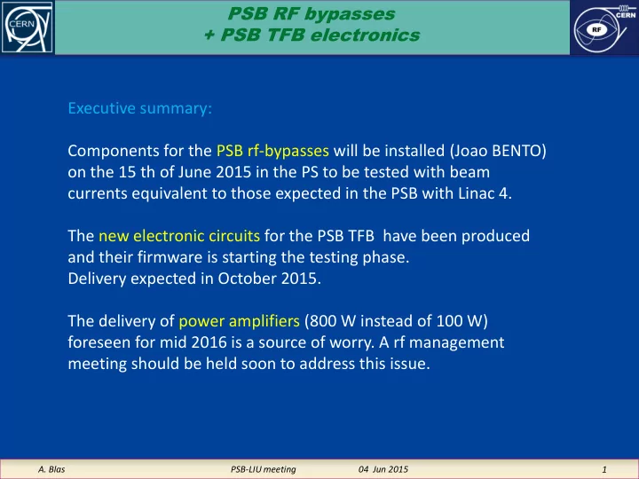
  17. PSB TFB electronics Firmware PSB TFB Digital Signal Processing = Saturation Betatron Phase CVORB detector decoder from CVORB Phase = Knob Observation point TFB PS Tune CVORB GENERAL = from CVORB decoder CONTROL LINK Tune to Phase LINK Tune Knob = Fonctionnal Block Loop Gain CVORB decoder from CVORB Gain Knob TFB Config. 50 MHz Upstream GAIN + Upstream clk h200 Clock Control + Dwnstr-1clk Revolution FIFO PU D ADC Betatron Automatic DAC OUT harmonics Clock domain 4L5 #1 Phase rotation Delay #1 Notch change Dwnstr-1 Upstream Upstream h64 Clock h64 Clock h64 Clock Non delayed h64 Clock Excitation Control Upstream Link h64 Clock C-Train + PS h1 Internal + Dwnstr-1 Clk Excitation source Transverse FIFO DAC Clock domain Excitation #2 Blow-up ADC change T.P. Excitation #3 Dwnstr-1 Upstream h64 Clock h64 Clock Tune FIFO Tune ADC DAC meas. Clock domain Excitation #4 #3 change Excitation T.P. PSB h1 DAC h1 clock Upstream Dwnstr-2 Clock #4 T.P. h64 Clock h64 Clock Dwnstr-2 Clk h64 A. Blas PSB-LIU meeting 04 Jun 2015 17

  18. PSB TFB electronics Conclusion Test in the PS of the new resistors to be used for PSB rf-bypasses from the 15 th of June 2015 onwards New low-level electronic circuits to be delivered in October 2015. 800 W power amplifiers progress is an issue requiring extraordinary measures. Not mentioned in the presentation: Tune value on a CVORB required for the operation of the new electronics Spare PU in the ring would be a good investment (instead of unused longitudinal PUs) A. Blas PSB-LIU meeting 04 Jun 2015 18

  19. Thank you! A. Blas PSB-LIU meeting 04 Jun 2015 19

  20. Appendix http://cds.cern.ch/record/447073/files/ps-2000-025.pdf http://cds.cern.ch/record/960437/files/cer-002626722.pdf http://indico.cern.ch/getFile.py/access?contribId=0&resId=1&materialId=slides&confId=59490 A. Blas PSB-LIU meeting 04 Jun 2015 20

  21. Appendix The Max peak beam intensity will be considered with 2.5E13 ppb and 130 ns bunch length = 3.14 ∙ 2.5 ∙ 10 13 ∙ 1.6 ∙ 10 −19 𝐽 𝑐𝑓𝑏𝑛 𝑞𝑓𝑏𝑙 𝑀𝑗𝑜𝑏𝑑 4 𝑏𝑢 𝑓𝑘 = 𝜇 𝑞𝑞 𝑓𝑘 = 𝜌 2 ∙ 𝑅 𝐶𝑣𝑜𝑑ℎ = 48𝐵 𝑞 260 ∙ 10 −9 𝑈 𝐶𝑣𝑜𝑑ℎ (The peak beam current in 2012 in the PS is 100 A p ) = 3.14 ∙ 2.5 ∙ 10 13 ∙ 1.6 ∙ 10 −19 𝐽 𝑐𝑓𝑏𝑛 𝑞𝑓𝑏𝑙 𝑀𝑗𝑜𝑏𝑑 4 𝑏𝑢 𝑗𝑜𝑘 = 𝜇 𝑞𝑞 𝑗𝑜𝑘 = 𝜌 2 ∙ 𝑅 𝐶𝑣𝑜𝑑ℎ = 15.7𝐵 𝑞 800 ∙ 10 −9 𝑈 𝐶𝑣𝑜𝑑ℎ A. Blas PSB-LIU meeting 04 Jun 2015 21

  22. Appendix 48 A p in a single 0.5 Ω resistor corresponds to 1152 W p and 24 V p In the nominal case, this current will be shared by the 3 bypasses => 16 A p (= 48/3) in each 0.5 Ω resistor corresponds to 128 W p and 8 V p For the resistance average power estimation it is reasonable to assume a centered beam => equally shared beam current The average beam current is for an average T REV = 1.425 MHz: 𝐽 𝐶𝑓𝑏𝑛 𝑒𝑣𝑠𝑗𝑜𝑕 𝑏𝑑𝑑𝑓𝑚𝑓𝑠𝑏𝑢𝑗𝑝𝑜 = 2.5 ∙ 10 13 ∙ 1.6 ∙ 10 −19 = 5.7 𝐵 𝑈 𝑆𝐹𝑊 For a 500 ms accelerating cycle within a 0.9 s cycle, the maximum average beam current will drop to: 𝐽 𝐶𝑓𝑏𝑛 𝑛𝑏𝑦−𝑀𝑗𝑜𝑏𝑑 4 = 3.1 𝐵 A. Blas PSB-LIU meeting 04 Jun 2015 22

  23. Appendix The average beam current at extraction with T REV = 546 ns: 𝐽 𝐶𝑓𝑏𝑛 𝑏𝑢 𝑓𝑦𝑢𝑠𝑏𝑑𝑢𝑗𝑝𝑜 = 2.5 ∙ 10 13 ∙ 1.6 ∙ 10 −19 = 7.3 𝐵 546 ∙ 10 −9 The average beam current at injection with T REV = 1000 ns: 𝐽 𝐶𝑓𝑏𝑛 𝑏𝑢 𝑗𝑜𝑘𝑓𝑑𝑢𝑗𝑝𝑜 = 2.5 ∙ 10 13 ∙ 1.6 ∙ 10 −19 = 4 𝐵 1000 ∙ 10 −9 A. Blas PSB-LIU meeting 04 Jun 2015 23

Download Presentation
Download Policy: The content available on the website is offered to you 'AS IS' for your personal information and use only. It cannot be commercialized, licensed, or distributed on other websites without prior consent from the author. To download a presentation, simply click this link. If you encounter any difficulties during the download process, it's possible that the publisher has removed the file from their server.

Recommend


More recommend