
SLIDE 1
4
IIT-Bombay Lecture 8 M. Shojaei Baghini
4
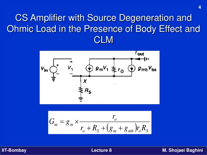
CS Amplifier with Source Degeneration and Ohmic Load in the Presence of Body Effect and CLM
( )
S
- mb
m S
- m
m
CS Amplifier with Source Degeneration and Ohmic Load in the Presence - - PowerPoint PPT Presentation
4 4 CS Amplifier with Source Degeneration and Ohmic Load in the Presence of Body Effect and CLM r = o G g ( ) + + + m m r R g g r R o S m mb o S IIT-Bombay Lecture 8
IIT-Bombay Lecture 8 M. Shojaei Baghini
S
m S
m
IIT-Bombay Lecture 8 M. Shojaei Baghini
s mb m s mb s mb m m v
m mb
IIT-Bombay Lecture 8 M. Shojaei Baghini
gs in
IIT-Bombay Lecture 8 M. Shojaei Baghini
IIT-Bombay Lecture 8 M. Shojaei Baghini
min 2 2 2 2 2 2 2 2 2 1 1 1
max max max
SGT DD b
in D THP in
D
TH
p bias DD
max 1 1 2
IIT-Bombay Lecture 8 M. Shojaei Baghini
1 2 |
TH GS DD in
1 2 3
TH GS DD GS in
IIT-Bombay Lecture 8 M. Shojaei Baghini
mb m in m mb D m D mb m v
IIT-Bombay Lecture 8 M. Shojaei Baghini