
SLIDE 1
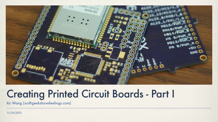
11/14/2012
Creating Printed Circuit Boards - Part I
Xo Wang (xo@geekshavefeelings.com)
Creating Printed Circuit Boards - Part I Xo Wang - - PowerPoint PPT Presentation
Creating Printed Circuit Boards - Part I Xo Wang (xo@geekshavefeelings.com) 11/14/2012 Hardware is hard But its not magic The process Design your entire project Fabricate Source Figure out why boards components it blew up Assemble
11/14/2012
Xo Wang (xo@geekshavefeelings.com)
But it’s not magic
Design your entire project Source components Fabricate boards Assemble prototype Figure out why it blew up
✤ Building hardware is an iterative cycle—
not a continuous process
✤ Each iteration tests concepts and exposes
problems
✤ Minimum costs of iterating a PCB ✤ >1 weeks of wait ✤ >10 hours of design/build/test ✤ >$100 out of pocket
✤ Combine parts into circuits ✤ Get parts from distributors like Digi-Key,
Mouser, Newark, etc.
✤ Every part has a data sheet—read it! ✤ For prototypes, you can connect parts on
a breadboard or perfboard
✤ Circuit boards used to be made by
drawing traces by hand and taping out photoresist mask
✤ Now we use ancient computer-aided
design (CAD) programs
✤ EAGLE, Cadence, Altium, Mentor ✤ Not so old: Fritzing, Circuits.io, Upverter
✤ A part/device in CAD is a footprint/
package together with a symbol
✤ Symbol is for your schematic ✤ Footprint/package is for your board ✤ Your library is a collection of devices
Library Device Footprint Symbol
✤ Your electrical design is your schematic ✤ Drawing a schematic in CAD is
schematic capture
✤ You draw nets to connect pins of
symbols together
✤ Be neat and document your work
because you’ll come back to this!
✤ The CAD program extracts a netlist of
nets to create a board layout
✤ You then lay out the components ✤ Note: the components are placed, but not
connected yet!
✤ You route the physical copper according
to your schematic design
✤ You draw traces of copper between
pads and/or through-holes
✤ Through-holes are usually plated on the
inside wall of the drill
✤ Vias are plated holes that switch sides
Via Trace (bottom) Trace (top)
✤ Your CAD program produces gerber
files, stripped design files (like a PDF)
✤ The fabrication house (fab) takes these
to produce a printed circuit board
✤ You (or laborers) assemble boards by
populating them with components
✤ More on fabrication in workshop Part III...
✤ Sparkfun tutorials & catalog ✤ Google for answers ✤ Ask us questions ✤ Give it a shot!
`
✤ Credit to Amanda Wozniak for her talk
“Hardware Will Cut You”
✤ Thanks to Greg Shikhman & Sterling Peet ✤ Arduino is a toy ✤ Hardware hacking ≠ hardware design ✤ Good luck; have fun!
`